Otsuka Clinic for Acupuncture, Osaka, Toyonaka, Hotarugaike, based on Japanese-style Traditional Chinese Medicine provides treatment for stiff shoulder, back pain, insomnia, hay fever, atopic dermatitis, beauty, infertility, childhood. English is available.

Menu


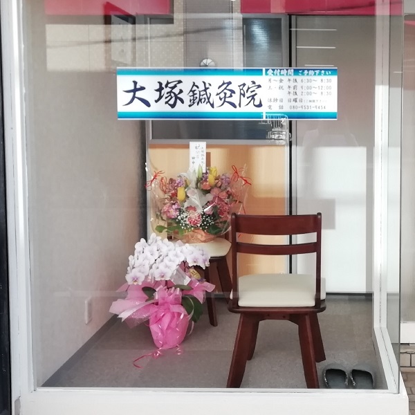
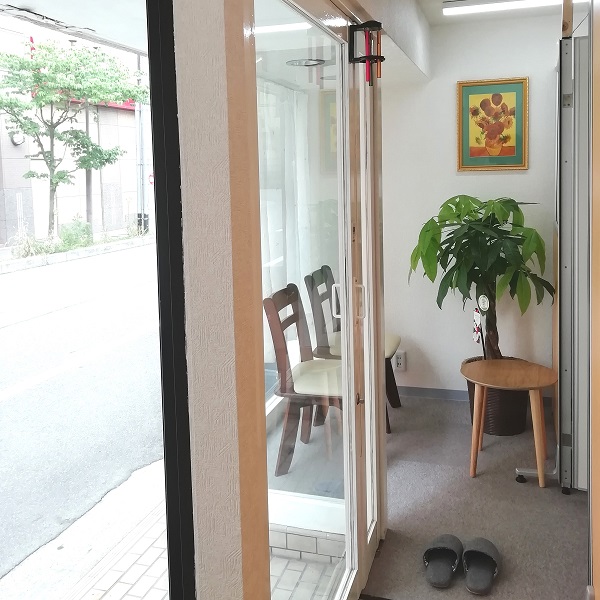
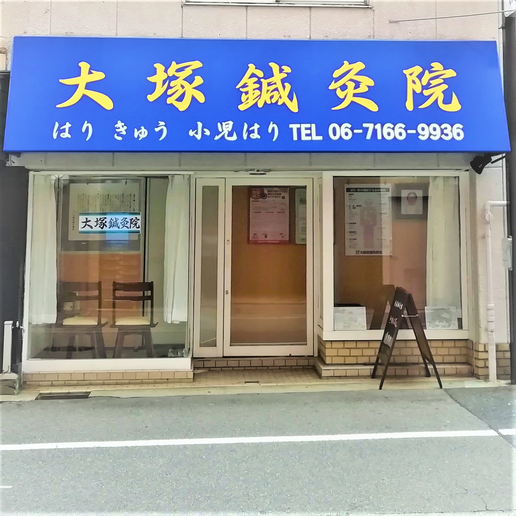
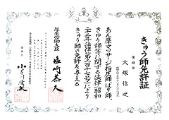
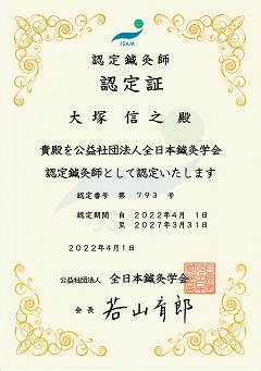
 What is Otsuka Clinic?

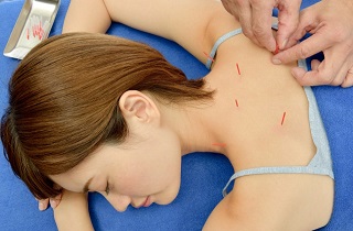
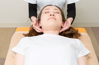
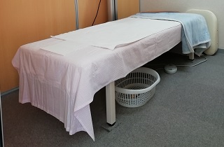
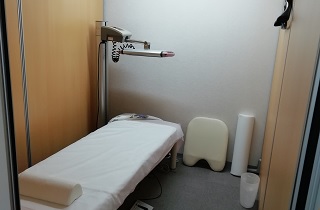
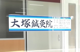
Otsuka Clinic is an acupuncture and moxibustion clinic in Toyonaka City.
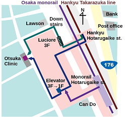
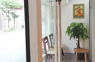
1 minute walk from Hotarugaike Station on the Hankyu Takarazuka Line.
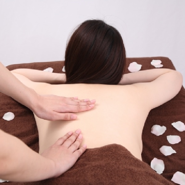
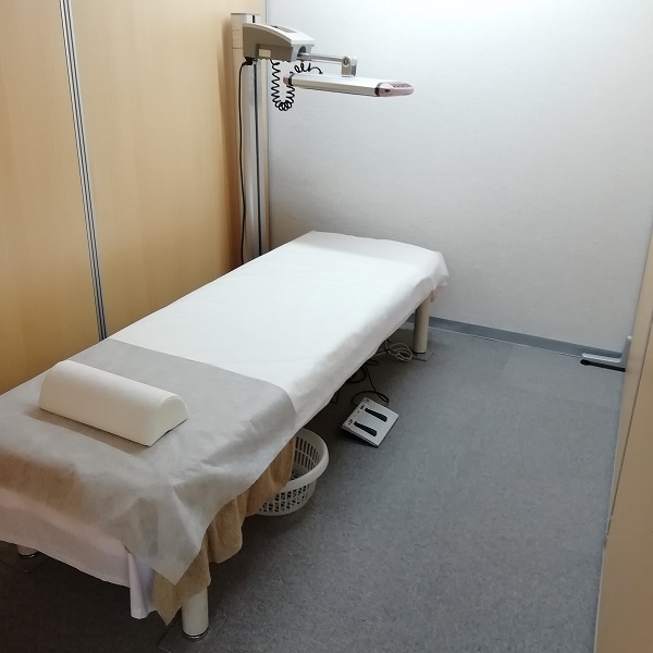
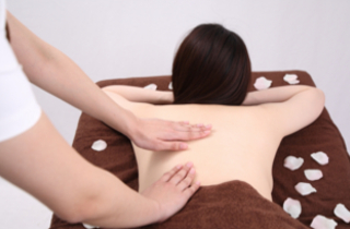
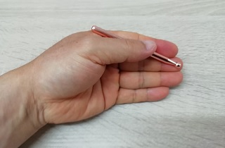
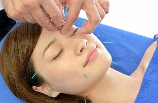
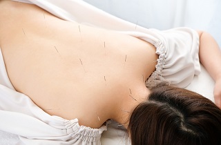
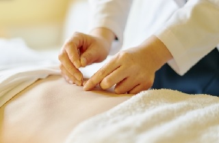
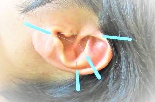
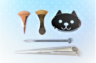
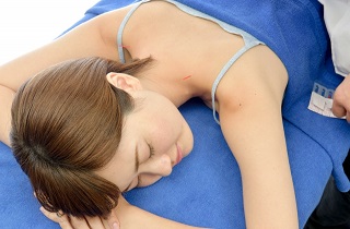
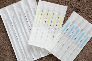
With painless Japanese-style acupuncture, you can enjoy a comfortable life.
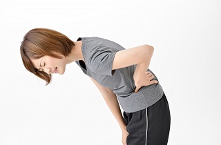
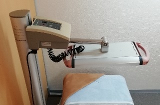
Acupuncture and moxibustion relieve muscle stiffness such as stiff shoulders and pain such as back pain.
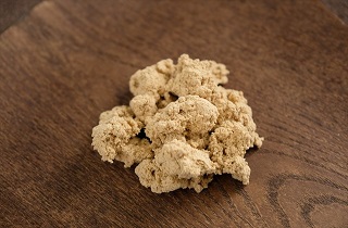
It will also relieve the pain of chronic fatigue and chronic illness.
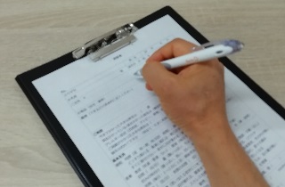
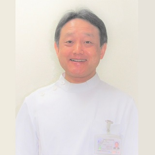
We will do everything in our power to help you live a symptom-free life.

 Nortification  

For safety treatment, hygiene measures are implemented.
Install disinfectant, Thoroughly clean and disinfect, Perform ventilation, Install an air purifier, Thoroughly wash hands and gargle, Wearing a mask, Thoroughly managing body temperature and physical condition, Eliminating contact between patients, Conducting prior interviews

October 21, 2023 Participated in National Convention of Japan Acupuncture and Moxibustion Association as a staff member

July 11, 2023 Interviewed on Otokoro.com (Posted at the bottom of the page)

June 10, 2023 Oral presentation at the Japan Society of Acupuncture and Moxibustion
"Heating characteristics of cone-shaped moxa at thermal threshold"

May 14, 2023 Participated in the academic seminar "Learning about Beauty Acupuncture from Harisienne"

May 12, 2023 Introduced on Otokoro.com

May 1, 2023 Started handling health insurance (Link to Japanese site)

March 10, 2023 Featured in "Recommended Acupuncture Clinics in Toyonaka City"

February 20, 2023 Listed on the website of the All Japan Acupuncture Society as a certified acupuncturist

February 6, 2023 Credit cards and electronic money can be used
Currently, Visa, Master, JCB, Amex, DC, Unionpay, iD, Q+, PayPay, d payment, auPAY, R Pay, Alipay, transportation electronic money (other than PiTaPa), etc.

Reasons for Choice

Why is your pain released and feeling better in Otska Clninic ?

If you find it hard to heal, it's too early to give up.
You have the option of Meridian Therapy based on Traditional Chinese Medicine at Otsuka Clinic.
Otsuka Clinic offers Japanese-style acupuncture and moxibustion treatments that are quite gentle on the body.

Three features why Otsuka Clinic is selected.

By improving your constitution, it is also effective for allergy, beauty, fertility, and mental worries.

Aligns the flow of meridians and enhances natural healing power.

The needle treatment is very shallow or only touches, so even beginners can rest assured.


RETURN

Reception Time

Reservation Priority !

Reception Time

Monday to Saturday & Public holiday
[Morning]      9:00 to 12:00
[Afternoon] 14:00 to 20:00
Closed day Sunday


MAP

1 minute on foot from Hotarugaike Station of
Hankyu Takarazuka line & Osaka monorail.

Directions

By Train or Monorail

Green:Stairs route
Blue :Elevator route

Behind the LUCIOLE

By Car

A parking space is available for one car on the right side facing Otsuka Clinic.
Only available during treatment.


RETURN

Reservation

How to reserve Otsuka Clinic?

Shinkyu Yoyaku

Reservation by Shinkyu Yoyaku is available.
Please make a reservation after registering as a member on the Shinkyu Yoyaku website.

Official LINE
Official LINE

You can apply for friends from LINE.
Please let us know your desired Date and Time by message.


RETURN

MENU

Carry out various treatments accourding to the symptoms.

Acu. & Moxa

Stimulates acupoints, improves blood circulation, enhances natural healing power and immunity.
Improves pain, coldness, swelling, malaise, menstrual cramps and other disorders.

Beauty Acu.

Promotes collagen production and increases tension and moisture.
Strengthens immunity, promotes blood flow and helps skin turnover.


Cupping

Creates clean blood and a stream of fresh oxygen.
Suppresses blood and stagnation, then improves physical deconditioning.


Shoulder & Scapula Adjustment

Relieves stiff shoulders, frozen shoulders, and pain and tenshion of neck, shoulders and back.
Physical conditions caused by stooping and headaches also improve.

Waist & Pelvic Adjustment

Restores the distorted skeleton and pelvis to a less burdensome state.
Improves back and knee pain.

Auricular Acupuncture

Adjusts the whole body with the ear points.
Stimulates the auricular acupuncture points after a full body treatment. Improves your physical condition and makes it easier to go on a diet.
Instead of needles, jewelry stickers can be applied. Jewelry hardly feels pain.

For children

To parents who are in trouble with their child's symptoms.
For your children such as crying at night, baby colic, and bedwetting.
Gently rubs the skin with a metal spatula. Children feel very comfortable.


RETURN


PRICE

Payment by credit card is available
Now, we accept VISA, Mastercard, and UnionPay

General course
Adults & College students
4,000JPY
3,500JPN for re-treatment within one month.
Initial visit takes 60-90 minutes
Re-treatment takes 40-60 minutes
Student course
Junior high school & High school students
3,000JPY
2,500JPN for re-treatment within one month.
Initial visit takes about 60 minutes
Re-treatment takes about 40 minutes
Children's course
Infants & Elementary school students
1,000JPY
Initial visit takes about 30 minutes
Re-treatment takes about 10 minutes

RETURN

For Beginners

Features of Otsuka Clinic & Mechanism of Acupuncture treatment.

Difference between Otsuka Clinic and others

Provideing painless and comfortable treatment and leading to drastic remedy.
Specialize in acupuncture and having full-body treatment.
Presenting the treatment plan and giving advice on your life.

Diseases being treated with Acupuncture

Effective not only for stiff shoulders and back pain, but also for various illnesses.
Internationally recognized as an alternative and complementary medicine.
Many disease cases and WHO indications are reported.

Mechanizm of Acupuncture Treatment

In acupuncture treatment, needles are used to move "Qi" existing in your body.
Improve blood flow and enhance natural healing power, then improve symptoms automatically on your own.

Meridian Therapy based on Pulse Diagnosis

In the pulse diagnosis of meridian therapy, the condition of the entire body is grasped using four diagnostic methods of oriental medicine, and the root cause of the symptoms is identified.
There are four diagnostic methods such as looking, listening, and asking diagnostics, and palpation.
In Otsuka Clinic, palpation is payed particular importance.


RETURN

Introduction of Otsuka Clinic

Treatment flow

Reception
Accepting reservations by reservation site, phone, or email.
Interview Sheet
Filling in the interview sheet based on your symptoms and worries.   PDF Download
Interview
Asking in detail about your symptoms and contents written in the interview sheet.
Outfit for Therapy
Adjusting clothes in order to treat your hands, feet, tummy, and back.

Palpation
Determine your pattern, which is the essence of the disease, by touching the condition of your abdominal region and pulsation.
Acu. Treatment
Based on the pattern, acupuncture needles are mainly use to adjust the whole body.

Explanation
Explaining the guideline for the next visit and the treatment plan.
Payment
Making a payment and your next reservation.

RETURN


Facilities

Needles

Hygienic disposable acupuncture needles are used.
Needles without insertion
Needles just touching without insertion are used.
Moxibustion

Using high quality domestically produced moxa.

Bed
Electric bed allows you use it at a reasonable height.
Infrared Heater
Warming your whole body and making you feel like sunbathing.
Private Treatment Space
The treatment space is a private room type surrounded by a wood grain partition.

RETURN

About Us

Overview of Otsuka Clinic

  Name Otsuka Clinic
  Address 3-8-14 Hotarugaike Nakamachi, Toyonaka, Osaka JAPAN
  President Dr. Nobuyuki Otsuka
  Access 1 minute on foot from Hotarugaike Station of Hankyu Takarazuka line & Osaka monorail.
  Parking A parking space for one car on the right side of the clinic.
  Phone Representative +81-671669936, Direct call +81-8095319454
  Email otsuka.clinic * otsuka.holding.jp
Please replace * with @.


RETURN

Career of President

 1962 Born in Onikubo, Uwa, Higashiuwa, Ehime, JAPAN.
 1985 Graduated from Tohoku University.
 1987 Completed doctoral program first semester at Tohoku University.
Joined Matsushita Electric Industrial Co., Ltd. and engaged in research as a researcher.
 1997 Received doctoral degree from Tohoku University.
At Telecommunications Advancement Organization of Japan, many co-authored papers were written with Professor Junichi Nishizawa.
 1999 Founded Hotal Ancient Medicine Research Institute as the representative.
 2017 Graduated from Meiji School of Oriental Medicine.
Recieved an acupuncture license and a moxibustion license.
Post-graduation clinical trainee at Meiji School of Oriental Medicine.
Established Otsuka Clinic, Togokuin at Kawanishi.
 2019 Established Otsuka Clinic, Keichiin at Toyonaka.
 2021 Retired Panasonic Corporation and dedicated to acupuncture and moxibustion treatment.
 2022 Recieved an honorific title of Certified Acupuncturist from The Japan Society of Acupuncture and Moxibustion.


RETURN

Qualification and Certification

License from Minister of Health, Labor and Welfare
Acupuncture license, Moxibustion license
Acupuncture license Moxibustion license


Certified Acupuncturist from The Japan Society of Acupuncture and Moxibustion
Certified Acupuncturist

Testimonial

Award for excellence from Japan College Association of Oriental Medicine

Award for excellence from Meiji School of Oriental Medicine

Research paper

Oriental medicine
Journal

●Nobuyuki Otsuka. Acupuncture and Moxibustion Therapy for Insomnia. Journal of Hotal Traditional Oriental Medicine. Vol.9, No.1, pp.1-15, 2022.
●Nobuyuki Otsuka. Acupuncture and Moxibustion Therapy for Tinnitus. Journal of Hotal Traditional Oriental Medicine. Vol.8, No.1, pp.1-9, 2021.
●Nobuyuki Otsuka. Acupuncture and moxibustion treatment for early detection of dementia. Journal of Hotal Traditional Oriental Medicine. Vol.7, No.1, pp.1-8, 2020.
●Nobuyuki Otsuka, Yumiko Handa. Ignition position dependence and skin absorption characteristics of light radiated from moxa needle. Journal of the Japan Society of Acupuncture and Moxibustion. Vol.70, No.1, pp.38-46, 2020.
●Nobuyuki Otsuka. A Case of Hands Numbness with Acupuncture and Moxibustion Treatment. Journal of Hotal Traditional Oriental Medicine. Vol.6, No.1, pp.1-6, 2019.
●Nobuyuki Otsuka. Acupuncture and Moxibustion Therapy for Infertility. Journal of Hotal Traditional Oriental Medicine. Vol.5, No.1, pp.1-10, 2018.
●Nobuyuki Otsuka. Acupuncture and Moxibustion Therapy for Diabetic Peripheral Neuropathy. Journal of Hotal Traditional Oriental Medicine. Vol.4, No.1, pp.1-9, 2017.
●Nobuyuki Otsuka. Acupuncture and Moxibustion Therapy for Chronic Fatigue Syndrome. Journal of Hotal Traditional Oriental Medicine. Vol.3, No.1, pp.1-9, 2016.
●Nobuyuki Otsuka. Pain Relief Effect of Acupuncture and Moxibustion Therapy. Journal of Hotal Traditional Oriental Medicine. Vol.2, No.1, pp.1-12, 2015.
●Nobuyuki Otsuka. Acupuncture and Moxibustion Therapy for Sports Injuries. Journal of Hotal Traditional Oriental Medicine. Vol.2, No.2, pp.1-13, 2015.
●Nobuyuki Otsuka. Pain of the Woman and Medical Treatment based on Western Medicine. Journal of Hotal Traditional Oriental Medicine. Vol.1, No.1, pp.1-3, 2014.
●Nobuyuki Otsuka. Acupuncture Relieves Menstrual Pain. Journal of Hotal Traditional Oriental Medicine. Vol.1, No.1, pp.4-6, 2014.
●Nobuyuki Otsuka. Acupuncture Relieves Dementing Disorder. Journal of Hotal Traditional Oriental Medicine. Vol.1, No.2, pp.1-5, 2014.
●Nobuyuki Otsuka. Acupuncture and Moxibustion Therapy Relieves Lower Urinary Tract Dysfunction. Journal of Hotal Traditional Oriental Medicine. Vol.1, No.3, pp.1-10, 2014.


Letters

●Nobuyuki Otsuka. Acupuncture and Moxibustion Treatment for Insomnia. Hotal Traditional Oriental Medicine Letters Vol.9, No.1, pp.1-8, 2022.
●Nobuyuki Otsuka. Acupuncture and Moxibustion Treatment for Tinnitus. Hotal Traditional Oriental Medicine Letters Vol.8, No.1, pp.1-6, 2021.
●Nobuyuki Otsuka. Acupuncture and Moxibustion Treatment for Early Detection of Dementia. Hotal Traditional Oriental Medicine Letters Vol.7, No.1, pp.1-6, 2020.
●Nobuyuki Otsuka. Acupuncture and Moxibustion Treatment for Hands Numbness. Hotal Traditional Oriental Medicine Letters Vol.6, No.1, pp.1-6, 2019.
●Nobuyuki Otsuka. Acupuncture and Moxibustion Treatment for Infertility. Hotal Traditional Oriental Medicine Letters Vol.5, No.1, pp.1-6, 2018.
●Nobuyuki Otsuka. Acupuncture and Moxibustion Treatment for Diabetic Neuropathy. Hotal Traditional Oriental Medicine Letters Vol.4, No.1, pp.1-4, 2017.
●Nobuyuki Otsuka. Acupuncture and Moxibustion Treatment for Chronic Fatigue Syndrome. Hotal Traditional Oriental Medicine Letters Vol.3, No.1, pp.1-5, 2016.
●Nobuyuki Otsuka. Findings on Chronic Pain Management. Hotal Traditional Oriental Medicine Letters Vol.2, No.1, pp.1-4, 2015.
●Nobuyuki Otsuka. Pain Relief Effect of Acupuncture and Moxibustion. Hotal Traditional Oriental Medicine Letters Vol.2, No.1, pp.5-10,2015.
●Nobuyuki Otsuka. Acupuncture and Moxibustion Treatment for Sports Injurie. Hotal Traditional Oriental Medicine Letters Vol.2, No.2, pp.1-5, 2015.
●Nobuyuki Otsuka. Pain of the Woman and Medical Treatment based on Western Medicine. Hotal Traditional Oriental Medicine Letters Vol.1, No.1, pp.1-2, 2014.
●Nobuyuki Otsuka. Acupuncture Relieves Menstrual Pain. Hotal Traditional Oriental Medicine Letters Vol.1, No.1, pp.3-4, 2014.
●Nobuyuki Otsuka. Acupuncture Relieves Dementing Disorder. Hotal Traditional Oriental Medicine Letters Vol.1, No.2, pp.1-4, 2014.
●Nobuyuki Otsuka. Acupuncture and Moxibustion Treatment Relieves Lower Urinary Tract Dysfunction. Hotal Traditional Oriental Medicine Letters Vol.1, No.3, pp.1-6, 2014.

Return


Electrical and Electronics

Doctoral Thesis
●Nobuyuki Otsuka. Research on fabrication of InP-based semiconductor lasers by metal-organic vapor phase epitaxy. Tohoku University (2017).

GaN Power Diodes, GaN MMICs
●Toshihide Ide, Mitsuaki Shimizu, Xu Qiang Shen, Hidetoshi Ishida, Masahiro Ishida, Nobuyuki Otsuka, Tetsuzo Ueda. Recovery current characteristics of diode mode operation in GaN gate injection transistor bi-directional switch. physica status solidi c, 14 (8) 1600245 (2017).
●Asamira Suzuki, Songbeak Choe, Yasuhiro Yamada, Nobuyuki Otsuka, Daisuke Ueda. NiO gate GaN-based enhancement-mode hetrojunction field-effect transistor with extremely low on-resistance using metal organic chemical vapor deposition regrown Ge-doped layer. Jpn. J. Appl. Phys., 55, 121001 (2016).
●Toshihide Ide, Mitsuaki Shimizu, Xu Qiang Shen, Tatsuo Morita, Nobuyuki Otsuka, Tetsuzo Ueda. High accuracy equivalent circuit model for GaN GIT bi-directional switch. physica status solidi c, 13 (5-6) 378-381 (2016).
●Shuichi Nagai, Yasuhiro Yamada, Noboru Negoro, Hiroyuki Handa, Miori Hiraiwa, Nobuyuki Otsuka, Daisuke Ueda. A 3-phase AC-AC matrix converter GaN chipset with drive-by-microwave technology. IEEE Journal of the Electron Devices Society, 3 (1) 7-14 (2015).
●Toshihide Ide, Ryousaku Kaji, Mitsuaki Shimizu, Kenji Mizutani, Hiroaki Ueno, Nobuyuki Otsuka, Tetsuzo Ueda, Tsuyoshi Tanaka. Evaluation of radiated emission of GaN-HEMT switching circuit. physica status solidi c, 11 (3-4) 936-939 (2014).
●S.Nagaia, Y.Yamadaa, Y. Kawaia, N. Negorob, H. Handab, M.Hiraiwaa, H.Uenoa, Y.Kudoha, K.Mizutania, M.Ishidab, T.Uedab, N.Otsuka, and D. Ueda. An Ultra Compact GaN 3x3 Matrix Converter. ECS Transactions, 64 (7) 41-49 (2014).
●N. Otsuka, S. Nagai, M. Yanagihara, U. Uemoto and D. Ueda. Low-Pressure Direct-Liquid-Cooling Technology for GaN Power Transistors. Jpn. J. Appl. Phys, Vol. 50 04DF07 (2011).
●N. Otsuka, S. Nagai, H. Ishida, Y. Uemoto T. Ueda, T. Tanaka, and D. Ueda. GaN Power Electron Devices. ECS Transactions, 41 (8) 51-70 (2011).

GaN Blue Laser Diodes and Ultraviolet Light-Emitting Diodes
●K. Harafuji, Y. Hasegawa, A. Ishibashi, A. Tsujimura, N. Otsuka, I. Kidoguchi, and Y. Ban. Complex Flow and Gas Phase Chemical Reactions in GaN MOVPE Reactor. Proc. Int. Workshop on Nitride Semiconductors, IPAP Conf.. Series 1 (2000) 101-104.
●A. Tsujimura, A. Ishibashi, Y. Hasegawa, S. Kamiyama, I. Kidoguchi, N. Otsuka, R. Miyanaga, G. Sugahara, M. Suzuki, M. Kume, K. Harafuji, and Y. Ban. Room-temperature CW operation of GaInN multiple quantum well laser diodes with optimized indium content. Phys. Status Solidi A 176 (1999) 53-57. 
●N. Otsuka, A. Tsujimura, Y. Hasegawa, G. Sugahara, M. Kume, and Y. Ban. 339 nm Deep-UV Emission from Al0.13Ga0.87N/Al0.10Ga0.90N Double Heterostructure Light-Emitting Diode on Sapphire Substrate. Proc. Int. Workshop on Nitride Semiconductors, IPAP Conf.. Series 1 (2000) 837-840.
●N. Otsuka, A. Tsujimura, Y. Hasegawa, G. Sugahara, M. Kume, and Y. Ban. Room Temperature 339 nm Emission from Al0.13Ga0.87N/Al0.10Ga0.90N Double Heterostructure Light-Emitting Diode on Sapphire Substrate. Jpn. J. Appl. Phys, 39 (2000) L445.

InP DFB lasers, InP strained MQW lasers
●N. Otsuka, M. Kito, Y. Yabuucni, M. Ishino, and Y. Matsui. Anomalous temperature dependence of PL characteristics in ordered InGaAsP strained layer multi-quantum well structure. Journal of Crystal Growth 170 (1997) 626-633.
●M. Ishino, N. Takaneka, M. Kito, K. Fujihara, N. Otsuka, K. Fujito, and Y. Matsui. Low distortion 1.3 μm strained-layer MQW-DFB laser for AM-SCM transmission systems with large channel capacity. J. Lightwave Technol. 15 (1997) 2172-2178.
●N. Otsuka, M. Kito, M. Ishino, and Y. Matsui. 1.5 μm strained-layer MQW-DFB lasers with high relaxation oscillation frequency and low chirp characteristics. IEEE J. Quantum Electron 32 (1996) 1230-1236.
●N. Otsuka, M. Kito, Y. Yabuucni, M. Ishino, and Y. Matsui. Degradation of PL characteristics in strained layer multi-quantum well structure with atomic ordering structure. Journal of Electronic Materials 25 (1996) 701-708.
●M. Kito, N. Otsuka, S. Nakamura, M. Ishino, and Y. Matsui. High-power, wide-temperature range operation of 1.3 μm gain-coupled DFB lasers with automatically buried InAsP absorptive grating. IEEE Photon. Technol. Lett. 8 (1996) 1299-1301.
●M. Kito, S. Kimura, N. Otsuka, K. Fujihara, M. Ishino, and Y. Matsui. High output power operation of 1.3 μm strained MQW lasers with low threshold currents at high temperature. Optical and Quantum Electron. 28 (1996) 503-511.
●M. Kito, S. Nakamura, N. Otsuka, M. Ishino and Y. Matsui. New structure of 1.3 μm strained-layer multi-quantum well complex-coupled distributed feedback lasers. Jpn. J. Appl. Phys. 35 (1996) 1375-1377.
●M. Kito, N. Otsuka, M. Ishino, and Y. Matsui. Barrier composition dependence of differential gain and external differential quantum efficiency in 1.3-μm strained-layer multiquantum-well lasers. IEEE J. Quantum Electron. 32 (1996) 38-42.
●N. Takenaka, M. Kito, N. Otsuka. Strained MQW-DFB laser module for broadband SCM transmission. National technical report 42(6) (1996) 708-713.
●M. Kito, H. Sato, N. Otsuka, N. Takenaka, M. Ishino, and Y. Matsui. Analysis of the second- and third-order intermodulation distortion in DFB lasers including dynamic spatial hole burning effect. IEEE Photon. Technol. Lett. 7 (1995) 144-146.
●N. Otsuka, M. Kito, Y. Mori, M. Ishino, and Y. Matsui. New structure by selective regrowth in multi-quantum well laser diodes performed by low pressure metalorganic vapor phase epitaxy. Journal of Crystal Growth 145 (1994) 866-874.
●M. Kito, N. Otsuka, M. Ishino, K. Fujihara, and Y. Matsui. Enhancement relaxation oscillation frequency of 1.3 μm strained-layer multiquantum well lasers. IEEE Photon. Technol. Lett. 6 (1994) 690-693.
●M. Kito, M. Ishino, N. Otsuka, N. Hoshino, K. Fujihara, K. Fujito, and Y. Matsui. Low distortion up to 2 GHz in 1.55 μm multiquantum well distributed-feedback laser. Electron. Lett. 28 (1992) 891-892.

Opto-Electronic Integrated circuit
●K. Matsuda, M. Kubo, N. Otsuka, and J. Shibata. Limitation factor of the bandwidth for InGaAs/InP monolithic photoreceiver. J. Lightwave Technology 7 (1989) 2059-2063.

Return


Solid-state physics

InP Molecular Layer Epitaxy
●N. Otsuka, J. Nishizawa, H. Kikuchi, and Y. Oyama. Expanded self-limiting growth condition of InP by alternate trimethylindium and tertiarybutylphosphine supply in ultrahigh vacuum. J. Crystal Growth 209 (2000) 252-257.
●N. Otsuka, J. Nishizawa, H. Kikuchi, and Y. Oyama. Self-limiting Growth Conditions on (001) InP by Alternate Triethylindium and Tertiarybutylphosphine Supply in Ultrahigh Vacuum. J. Vac. Sci. Technol. A17 (1999) 3008-3018.
●N. Otsuka, J. Nishizawa, H. Kikuchi, and Y. Oyama. Self-limiting growth of InP by alternate trimethylindium and tertiarybutylphosphine supply in ultrahigh vacuum. J. Crystal Growth 205 (1999) 253-263.
●N. Otsuka, J. Nishizawa, H. Kikuchi, and Y. Oyama. Self-limiting submonolayer growth of InP by alternative triethylindium and tertiarybutylphosphine supply in ultra high vacuum. Inst. Phys. Conf. Ser 162 (1999) 529-534.
●N. Otsuka, J. Nishizawa, H. Kikuchi, and Y. Oyama. Self-Limiting Growth of Specular InP Layer by Alternate Injection of Triethylindium and Tertiarybutylphosphine in Ultrahigh Vacuum. Jpn. J. Appl Phys. 38 (1999) L20-L23.

InP Self-limiting Etching
●N. Otsuka, J. Nishizawa, Y. Oyama, H. Kikuchi, and K. Suto. Self-limiting etching prior to self-limiting growth in ultra-high vacuum for obtaining clean interface. International Conference for The Physics of Semiconductors (2001) .
●N. Otsuka, J. Nishizawa, Y. Oyama, H. Kikuchi, and K. Suto. Digital Etching of InP by Intermittent Injection of Phosphorous Precursors in Ultra-high Vacuum. Jpn. J. Appl Phys. 38 (1999) 2529-2537.
●N. Otsuka, J. Nishizawa, Y. Oyama, H. Kikuchi, and K. Suto. Digital etching of InP by intermittent injection of tris-dimethylaminophosphorus in ultra high vacuum. J. Electrochem. Soc.. 146 (1999) 547-550.
●N. Otsuka, Y. Oyama, H. Kikuchi, J. Nishizawa, and K. Suto. Digital etching of (001) InP substrate by intermittent injection of tertiarybutylphosphine in ultrahigh vacuum. Jpn. J. Appl Phys. 37 (1998) L1509-L1512.

InP MOVPE growth
●N. Otsuka, M. Ishino, and Y. Matsui, F. Toujou. Control of double diffusion front unintentionally penetrated from a Zn doped InP layer during metalorganic vapor phase epitaxy. J. Appl. Phys. 84 (1998) 4239-4247.
●N. Otsuka, M. Ishino, and Y. Matsui. Stability of Zn doping profile in modulation doped multiple quantum well structure. J. Appl. Phys. 80 (1996) 1405-1413.
●M. Shiojiri, T. Isshiki, K. Nishino, M. Tsujikura, J. Saijo, Y. Takahashi, N. Ohtsuka, and Y. Yabuuchi. Quantitative Structure Images of Interfaces in InGaAs/InP Multilayer Heterostructures. J. Electron Microsc 41 (1992) 434-444. and Ultramicroscopy.
●Y. Yabuuchi, Y. Takahashi, N. Ohtsuka, T. Isshiki, M. Tsujikura, H. Saijo, and M. Shiojiri. High-Resolution Transmission Electron Microscopy Observations of InGaAs/InP Multilayer Heterostructures. Phys. Stat. Sol. (a) 127 (1991) 385-396.

Mg2Si1-xGex compound semiconductors
●Y. Noda, H. Kon, Y. Furukawa, N. Otsuka, I. Nishida, and K. Masumoto. Preparation and thermoelectric properties of Mg2Si1-xGex (x=0.0~0.4) solid solution semiconductors. Materials Transactions, JIM 33 (1992) 845-850.
●Y. Noda, N. Otsuka, K. Masumoto, and I. Nishida. Preparation of thermoelectric properties of Mg2Si1-xGex solid-solution semiconductor. Nippon Kinzoku Gakkai-si 53(5) (1989) 487-493.

Return


Proceedings


Oriental medicine

●Nobuyuki Otsuka, Yumiko Handa. A study of acupuncture and moxibustion effect using time series analysis on body weight. The Japan Society of Acupuncture and Moxibustion (jsam) 2022 Abstruct No.037. pp.162, 2022.
●Nobuyuki Otsuka, Yumiko Handa. Moxa hight dependence of combustion characteristics and heating effect of thermosensitive moxibustion. The Japan Society of Acupuncture and Moxibustion (jsam) 2021 Abstruct No.005. pp.128, 2021.
●Nobuyuki Otsuka. Moxa structural dependence of combustion characteristics and heating effect of thermosensitive moxibustion. Journal of the Japan Society of Acupuncture and Moxibustion. Vol.70, No.3, pp.156, 2020.
●Nobuyuki Otsuka, Yumiko Handa. Skin absorption characteristics of the light radiated from moxa needle. The Japan Society of Acupuncture and Moxibustion (jsam) 2019 Abstruct No.217 2-P-I(4). pp.236, 2019.
●Nobuyuki Otsuka. Acupuncture and Moxibustion are effective for Inguinal Hernia: a case report. The Japan Society of Acupuncture and Moxibustion (jsam) 2018 Abstruct No.129 2-P-E1(2). pp.224, 2018.

Return


Electrical and Electronics

GaN Power devices, GaN MMICs
●D. Ueda, M. Hikita, S. Nakazawa, K. Nakazawa, H. Ishida, M. Yanagihara, K. Inoue, T. Ueda, Y. Uemoto, T. Tanaka, N. Otsuka and Takashi Egawa, " GaN-Based Power Devices", in Tech Digest of International Symposium on Advanced Nanodevices and Nanotechnology 2009 (ISANN2009) (Kaanapali, Maui, Hawaii, USA, November 29-December 4, 2009).
●N. Otsuka, S. Nagai, M. Yanagihara, U. Uemoto and D. Ueda " Direct Liquid Cooling Technology for Power Semiconductor Devices " in Extended Abstracts of the 2010 International Conference on Solid State Devices and Materials, Tokyo, 2010, pp1229-1230.
●(Invited) N. Otsuka, S. Nagai, H. Ishida, Y. Uemoto T. Ueda, T. Tanaka, and D. Ueda "GaN Power Electron Devices" in Extended Abstracts of the 220th ECS Meeting, Electrochemical Society, Boston, 2011, Abstract #2170.
●K. Mizutani, H. Ueno, Y. Kudoh, S. Nagai, K. Inoue, N. Otsuka, T. Ueda, T. Tanaka and D. Ueda "Integrated Power Design Platform based on Modeling Dynamic Behavior of GaN Devices, in Technical Digest of the IEDM 2011, 2011 IEEE International Electron Devices Meeting, Washington, DC, 2011, 26.4.1.
●S. Nagai, T. Kojima, M. Koyama, T. Shiraishi, Y. Kudoh, N. Otsuka, A. Ikoshi, Y. Uemoto, T. Ueda, T. Tanaka, K. Inoue and D. Ueda " An Ultra Compact Dual-Side Cooled Surface Mount GaN Multi-chip Inverter Package with Cu Leads Direct Bonding" in Abstract of the 9th Topical Workshop on Heterostructure Microelectronics , TWHM 2011, Gifu, 2011, 103.
●(Invited) K. Mizutani, H. Ueno, Y. Kudoh, S. Nagai, K. Inoue, N. Otsuka, T. Ueda, T. Tanaka and D. Ueda "Integrated Power Design Platform for Power Electronics Applications with GaN Devices" in Workshop Digest of the AWAD 2012, 2012 Asia-Pacific Workshop on Fundamentals and Applications of Advanced Semiconductor Devices, Okinawa, 2012, 302.
●R. Baert, M. Badaroglu, K. Mizutani, H. Ueno, Y. Kudoh, S. Nagai, K. Inoue, N. Otsuka, and D. Ueda "Fast Simulation of Power Electronic Systems by Partitioning, Segmentation and Caching" in Abstract of 13th IEEE Workshop on Control and Modeling for Power Electronics, COMPEL'12, 2012, Kyoto.
●(Invited) N. Otsuka, "GaN Power Electron Devices" International SiC Power Electronics Applications Workshop, ISiCPEAW2012, Stockholm, 2012.
●S. Nagai, N. Negoro, T. Fukuda, H. Sakai, T. Ueda, T. Tanaka, N. Otsuka and D. Ueda "Drive-by-Microwave Technologies for Isolated Direct Gate Drivers" in Proceeding of 2012 IEEE MTT-S International Microwave Workshop Series (IMWS) on Innovative Wireless Power Transmission: Technologies, Systems, and Applications, IMWS-IWPT2012, Kyoto, 2012, 267-270.
●S. Nagai, N. Negoro, T. Fukuda, N. Otsuka, H. Sakai, T. Ueda, T. Tanaka and D. Ueda "A DC-Isolated Gate Drive IC With Drive-by-Microwave Technology for Power Switching Devices" in Proceeding of 2012 IEEE International Solid-State Circuits Conference, ISSCC 2012, San Francisco, 2012, 404-406.
●S. Nagai, T. Fukuda, N. Otsuka, D. Ueda , N. Negoro, H. Sakai, T. Ueda, T. Tanaka "A One-chip Isolated Gate Drive with an Electromagnetic Resonance Coupler Using a SPDT switch" in Proceeding of the 2012 24th International Symposium on Power Semiconductor Devices and ICs, ISPSD 2012, Bruges, 2012, 73-76.
●(Invited) D. Ueda , N. Otsuka, S. Nagai, N. Negoro, T. Fukuda, H. Sakai, T. Morita, T. Ueda, T. Tanaka "A Novel Insulated GaN Gate-Driver with Wireless Power Transfer Technology", in abstract of the International Workshop on Nitride Semiconductors 2012, IWN2012, Sapporo, 2012,
●(Invited) N. Otsuka, " Recent Progress on GaN-based Power Devices " International Workshop on Wide-Band-Gap Power Electronics 2013, IWWPE2013, Hsinchu, 2013.
●A. Suzuki, Y. Yamada, H. Tanaka, H. Ueno, N. Otsuka, Y. Anda, T. Ueda, T. Tanaka, and D. Ueda, "Low on-state resistance normally-off AlGaN/GaN HFET with ALD formed p-type NiO Gate", in proceedings of the 37th workshop on compound semiconductor devices and integrated cirquits, WOCSDICE 2013, Warnemunde, 2013.
●Toshihide Ide, Ryousaku Kaji, Mitsuaki Shimizu, Kenji Mizitani, Hiroaki Ueno, Nobuyuki Otsuka , Tetsuzo Ucda and Tsuyoshi Tanaka "Evaluation of Radiated Emission of GaN-HEMT Switching Circuit.", in abstract of 10th International Conference on Nitride Semiconductors 2013, ICNS-10, Washington, D.C., 2013, 31, DP3.08
●(Invited) N. Otsuka, " Recent Progress in GaN Power Devices " The 6th International Symposium on Advanced Plasma Science and its Applications for Nitrides and Nanomaterials, ISPlasma2014, Nagoya, 2014.
●Yuji Kudoh, Nobuyuki Otsuka, Kenji Mizutani, Toshimitsu Morizane “A Novel Single to Two-Phase Matrix Converter for Driving A Symmetrically Designed Two-Phase Induction Motor”, IEEE 10th International Conference on Power Electronics and Drive Systems (PEDS), 2013, April, 1133-1138.
●S. Nagai, Y. Yamada, N. Negoro, H. Handa, Y. Kudoh, H. Ueno, M. Ishida, N. Otuska, D. Ueda ” A GaN 3×3 Matrix Converter Chipset with Drive-by-Microwave Technologies” 2014 IEEE International Solid-State Circuits Conference, 30.5
●Yuji Kudoh, Kenji Mizutani, Nobuyuki Otsuka, Satoru Takahashi, Masahiko, Inamori, Hiroto Yamagiwa, Tatsuo Morita, Tetsuzo Ueda, Tsuyoshi Tanaka, Daisuke Ueda, Toshimitsu Morizane, “Single to 2-phase Matrix Converter using GaN-based Monolithic Bidirectional Switch for Driving Symmetrical 2-phase Motor” IEEE Energy Conversion Congress and Exhibition (ECCE 2014) P7103.
●A. Suzuki, S. Choe, Y. Yamada, S. Nagai, M. Hiraiwa, N. Otsuka. D. Ueda “Extremely low on-resistance enhancement-mode GaN-based HFET using Ge-doped regrowth technique”, Electron Devices Meeting, IEDM (2014).
●Tetsuya Yamamoto; Tetsuro Sawai; Kenji Mizutani; Nobuyuki Otsuka; Eiji Fujii; Nobuyuki Horikawa; Yoshihiko Kanzawa, “A novel duality-based modeling methodology for reverse current-voltage characteristics of SiC”, 2014 International Conference on Simulation of Semiconductor Processes and Devices (SISPAD), pp. 53-55 (2014).
●Daisuke Ueda; Takeshi Fukuda; Shuichi Nagai; Hiroyuki Sakai; Nobuyuki Otsuka; Tatsuo Morita; Noboru Negoro; Tetsuzo Ueda; Tsuyoshi Tanaka, “Present and Future of GaN Power Devices”, CIPS 2014; 8th International Conference on Integrated Power Electronics Systems, pp. 1-5 (2014).
●Shuichi Nagai; Yasufumi Kawai; Osamu Tabata; Hideaki Fujiwara; Nobuyuki Otsuka; Daisuke Ueda; Noboru Negoro; Masahiro Ishida, “A compact Drive-by-Microwave gate driver with coupler integrated in a package”, 2014 IEEE Applied Power Electronics Conference and Exposition - APEC 2014, pp. 1461 - 1464 (2014).
●Shuichi Nagai; Yasufumi Kawai; Osamu Tabata; Hideaki Fujiwara; Noboru Negoro; Masahiro Ishida; Nobuyuki Otsuka, “A Drive-by-Microwave isolated gate driver with gate current charge for IGBTs”, 2014 16th European Conference on Power Electronics and Applications, pp. 1 - 6 (2014).
●Shuichi Nagai; Yasufumi Kawai; Osamu Tabata; Hideaki Fujiwara; Yasuhiro Yamada; Nobuyuki Otsuka; Daisuke Ueda; Noboru Negoro; Masahiro Ishida, “A Drive-by-Microwave isolated gate driver with a high-speed voltage monitoring”, 2014 IEEE 26th International Symposium on Power Semiconductor Devices & IC's (ISPSD) 434-437 (2014).
●Yasufumi Kawai; Shuichi Nagai; Osamu Tabata; Hideaki Fujiwara; Noboru Negoro; Hiroaki Ueno; Masahiro Ishida; Nobuyuki Otsuka “An isolated DC power supply free compact GaN inverter module”, 2015 IEEE 11th International Conference on Power Electronics and Drive Systems, pp. 84-88 (2015).
●(Invited) Nobuyuki Otsuka; Yasufumi Kawai; Shuichi Nagai “Recent progress in GaN devices for power and integrated circuit”, 2017 IEEE 12th International Conference on ASIC (ASICON), pp. 928 - 931 (2017).

GaN Blue Laser Diodes and Ultraviolet Light-Emitting Diodes
●N. Otsuka, A. Tsujimura, Y. Hasegawa, G. Sugahara, M. Kume, and Y. Ban “339 nm Deep-UV Emission from Al0.13Ga0.87N/Al0.10Ga0.90N Double Heterostructure Light-Emitting Diode on Sapphire Substrate”, in Tech Digest of International Workshop on Nitride Semiconductors (IWN2000) (Nagoya, Japan, 2000) paper WM1-2, pp. 114.
●K. Harafuji, Y. Hasegawa, A. Ishibashi, A. Tsujimura, N. Otsuka, I. Kidoguchi, and Y. Ban “Complex Flow and Gas Phase Chemical Reactions in GaN MOVPE Reactor”, in Tech Digest of International Workshop on Nitride Semiconductors (IWN2000) (Nagoya, Japan, 2000) paper PMD-22, pp. 172.

InP DFB lasers, InP strained MQW lasers
●N. Otsuka, M. Ishino, M. Kito, K. Hoshino, K. Fujihara, K. Fujito, and Y. Matsui, "Low distortion over wide-band modulation of 1.55-?m MQW distributed-feedback lasers", in Tech Digest of Optical Fiber Communication Conference '92 (San Jose, California, 1992) Paper FB5, pp. 275.
●N. Otsuka, M. Ishino, K. Fujihara, M. Kito, Y. Mori, H. Sato, and Y. Matsui, "Low-chirp characteristics over wide-band modulation of multiple-quantum-well distributed-feedback lasers", in Tech Digest of 9th International Conference on Integrated Optics and Optical Fiber Communication '93 (San Jose, California, 1993) Paper WH15, pp. 127-128.
●N. Otsuka, M. Kito, Y. Mori, M. Ishino, and Y. Matsui, "New structure by selective regrowth in MQW laser diodes performed by low pressure MOVPE", in Proc. 7th International Conference on Metalorganic Vapor Phase Epitaxy (Yokohama, Japan, 1994) Paper P3-2, pp. 268-269.
●N. Otsuka, M. Kito, Y. Yabuucni, M. Ishino, and Y. Matsui, "Atomic ordering in strained layer multi-quantum well structure", in Proc. 7th International Conference on Indium Phosphide and Related Materials (Sapporo, Japan, 1995) Paper FA1.4, pp. 701-704.
●N. Otsuka, M. Kito, M. Ishino, and Y. Matsui, "1.5 ?m strained-layer MQW-DFB lasers with low chirp and low distortion characteristics", in Tech Digest of 10th International Conference on Integrated Optics and Optical Fiber Communication '95 (Hong Kong, 1995) Paper FB2-6, pp. 50-51.
●N. Otsuka, M. Kito, Y. Yabuucni, M. Ishino, and Y. Matsui, "Anomalous temperature dependence of PL characteristics in ordered InGaAsP strained layer multi-quantum well structure", in Proc. 8th International Conference on Metalorganic Vapor Phase Epitaxy (Weales, England, 1996) Paper OSSP.6.
●M. Ishino, K. Fujihara, N. Otsuka, N. Takenaka, T. Uno, and Y. Matsui, “High performance analog transmission characteristics of 1.3 ?m wavelength multiquantum well distributed feedback laser,” in Tech Digest of Optical Fiber Communication Conference '91 (San Diego, California, 1991) Paper WG6, pp. 93.
●M. Kito, N. Otsuka, K. Fujihara, S. Yamane, M. Ishino, K. Fujito, and Y. Matsui, “Extremely low bias current operation of 1.3 ?m strained-layer MQW-DFB laser for 97 ch AM-FDM transmission,” in Extended Abstract 1993 International Conference Solid State Devices and Materials (Chiba, Japan,1993) Paper D-6-4, pp. 1035-1037.
●K. Fujihara, Y. Mori, M. Kito, N. Otsuka, M. Ishino, and Y. Matsui, “High characteristics temperature 1.48?m strained-layer MQW laser diode with wide bandgap barrier layers,” IEDM ‘93 (Wasnington, D.C., 1993) Paper 23.5, pp. 605-608.
●M. Ishino, M. Kito, S. Yamane, K. Fujihara, N. Otsuka, H. Sato, and Y. Matsui, “1.3 ?m strained-layer MQW-DFB laser with low noise and low distortion characteristics for 100-channel CATV transmission,” in Tech Digest of International Electron Devices Meeting 1993 (Washington, DC., 1993) Paper 23.7, pp. 613-616.
●M. Kito, H. Sato, N. Otsuka, N. Takenaka, M. Ishino and Y. Matsui, “The effect of dynamic spatial hole burning on the second and third order intermodulation distortion in DFB lasers,”in Proc. 14th IEEE Int. Semiconductor Laser Conf. (Maui, Hawaii, 1994) Paper T2.6, pp. 57-58.
●M. Kito, H. Sakai, N. Otsuka, K. Fujihara, M. Ishino and Y. Matsui, “High output power operation of 1.3 ?m strained MQW lasers with low threshold currents at high temperature,” in Proc. 7th International Conference on Indium Phosphide and Related Materials (Sapporo, Japan, 1995) Paper ThP37, pp. 508-511.
●M. Kito, S. Nakamura, N. Otsuka, M. Ishino and Y. Matsui, “Novel structure of 1.3 ?m strained-layer MQW complex-coupled DFB lasers,” in Extended Abstract 1995 International Conference Solid State Devices and Materials (Osaka, Japan, 1995) Paper D-4-3, pp. 431-433.
●M. Kito, N. Otsuka, S. Nakamura, M. Ishino and Y. Matsui, “High-power, wide-temperature range operation of 1.3-?m complex-coupled DFB lasers with automatically buried absorptive grating,” in Tech Digest of Optical Fiber Communication ‘96, (San Jose, California, 1996) Paper TuH5, pp. 38-39.
●J. Ohya, N. Otsuka, S. Nakamura, Y. Inaba, M. Ishino, Y. Matsui, M. Fuse, K. Nojima, Y. Ishii, S. Kawashima, and S, Kitaji, “Low noise and low distortion AM/FM converter with frequency modulated 1.55?m strained-layer MQW-DFB laser for analog transmission,” in Tech Digest of 11th international conference on Integrated Optics and Optical Fiber Communications/23rd European Conference on Optical Communications, (Edinburgh, UK, 1997) pp. 94-97.

Opto-Electronic Integrated circuit
●N. Otsuka, K. Matsuda, and J. Shibata, "InGaAs/InP Monolithic Array Photoreceiver Consisting of 10 PIN/FET's", in Tech Digest of 7th International Conference on Integrated Optics and Optical Fiber Communication '89 (Kobe, Japan, 1989) Paper 20C4-1, pp. 166-167.

Return


Solid-state physics

InP Molecular Layer Epitaxy
●N. Otsuka, J. Nishizawa, H. Kikuchi, and Y. Oyama, “Self-limiting submonolayer growth of InP by alternative triethylindium and tertiarybutylphosphine supply in ultra high vacuum,” in Tech Digest of 25th International Symposium on Compound Semiconductors (ISCS'98), (Nara, Japan, 0998) paper TuP-2.
●N. Otsuka, J. Nishizawa, H. Kikuchi, and Y. Oyama, “Extended self-limiting growth condition of InP using alternate trimethylindium and tertiarybutylphosphine supply in ultrahigh vacuum,” in Tech Digest of 7th International Conference on Chemical Beam Epitaxy and Related Growth Techniques (ICCBE’99), (Tsukuba, Japan, 1999) paper We3-8.

InP Self-limiting Etching
●N. Otsuka, J. Nishizawa, Y. Oyama, H. Kikuchi, and K. Suto, “Digital etching of InP using tris-dimethylaminophosphorus in ultra-high vacuum,” in Tech Digest of 1998 International Conference on Solid-State Devices and Materials (SSDM'98), (Hiroshima, Japan, 1998) paper D-4-6, pp.238.
●N. Otsuka, J. Nishizawa, Y. Oyama, H. Kikuchi, and K. Suto, “Self-limiting etching prior to self-limiting growth in ultra-high vacuum for obtaining clean interface,” in Tech Digest of 25th International Conference for The Physics of Semiconductors (ICPS25), (Osaka, Japan, 2000) paper D052.

InP MOVPE growth
●Y. Yabuuchi, Y. Takahashi, N. Otsuka, T. Isshiki, K. Nishio, M. Tsujikura, H. Saijo, and M. Shiojiri, “HRTEM of heterointerfaces in InGaAs/InP multilayer crystals,” in proc. 5th Asia-Pacific Electron Microscopy Conference (Beijin, China, 1992) pp. 572-573.
●Y. Yabuuchi, Y. Takahashi, N. Otsuka, T. Isshiki, K. Nishio, M. Tsujikura, H. Saijo, and M. Shiojiri, “HRTEM images of InGaAs/InP multilayer heterostructures,” in proc. 10th European Congress on Electron Microscopy (Gramada, Spain, 1992) pp. 167-168.

Return


Publications

●Nobuyuki Otsuka. Modern kana notation Shinkyu-tyouhouki-koumoku. 蛍東洋医学研究所 (2022).
●Nobuyuki Otsuka. Translated by Hotal Ancient Medicine Research Institute Shindou-hiketsu-syu. 蛍東洋医学研究所 (2021).
●Nobuyuki Otsuka, Shuichi Nagai, Daisuke Ueda. Power Device Packaging Technology, Chapter 4. Science & Technology, 239-262 (2012).

Return