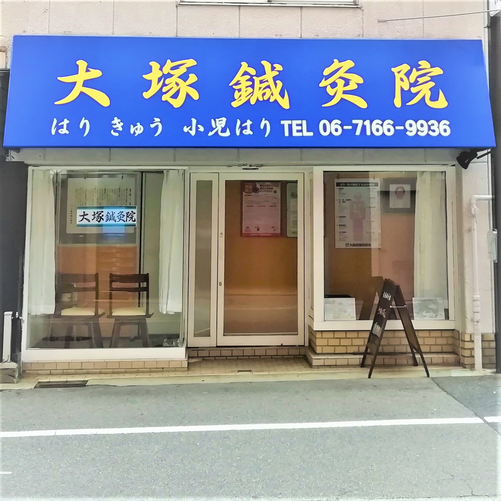
什么是大塚针灸诊所?
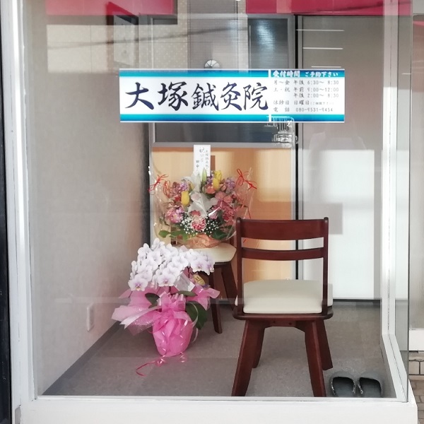
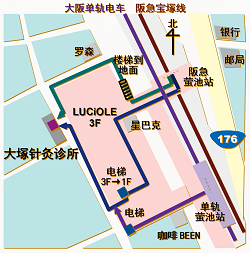
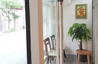
大塚针灸诊所位于丰中市内。距离阪急宝冢线萤池站步行一分钟。
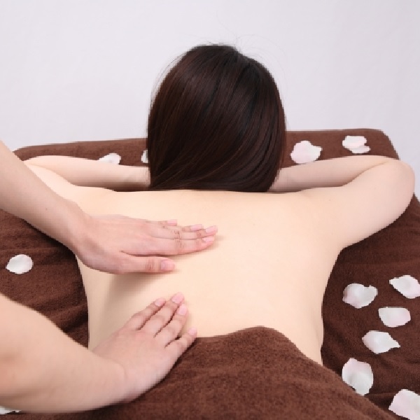
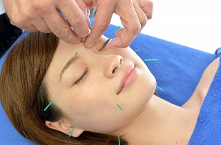
采用无痛日式针灸,助您享受舒适的生活。
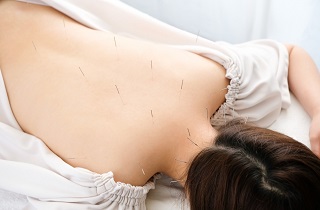
针灸可缓解肩部等肌肉僵硬和背部等疼痛。还能减轻慢性疲劳和慢性疾病带来的苦痛。
我们将竭尽全力帮助您缓解症状治愈疾病,从而改善您的生活。
什么是大塚针灸诊所?
大塚针灸诊所位于丰中市内。距离阪急宝冢线萤池站步行一分钟。
采用无痛日式针灸,助您享受舒适的生活。
针灸可缓解肩部等肌肉僵硬和背部等疼痛。还能减轻慢性疲劳和慢性疾病带来的苦痛。
我们将竭尽全力帮助您缓解症状治愈疾病,从而改善您的生活。
通知
彻底的卫生措施
安装消毒剂、彻底清洁消毒、通风、安装空气净化器、彻底洗手、戴口罩、并进行我们彻底管理体温和身体状况
为什么在大塚针灸诊所可以去除骨科、按摩科无法治愈的疼痛,改善身体状况?

如果你发现很难治愈,现在就放弃还为时过早。
在大塚针灸诊所,您可以选择基于脉诊流经络治疗。
大塚诊所提供对身体相当温和的日式针灸治疗。


预约优先!
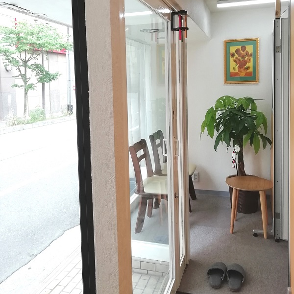
从阪急宝冢线、大阪单轨电车萤池站步行1分钟
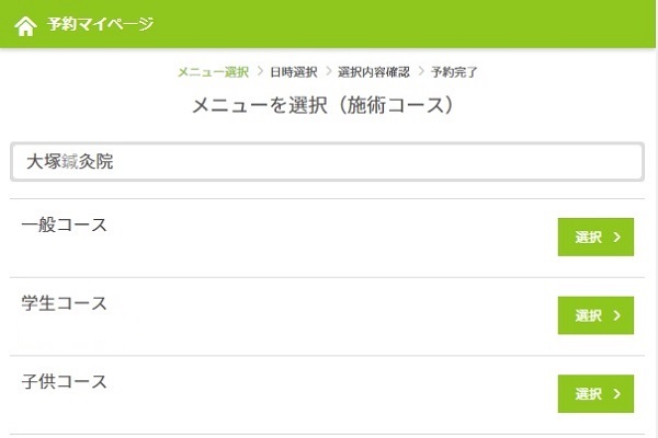
预订方法如下
我们会根据您的症状和需要对您进行治疗

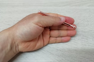
针和灸是我们医院的基础。
它刺激压力点,改善血液循环,增强自然愈合能力和免疫力。它不仅可以减轻疼痛,还可以改善感冒、肿胀、全身不适和月经来潮等症状。
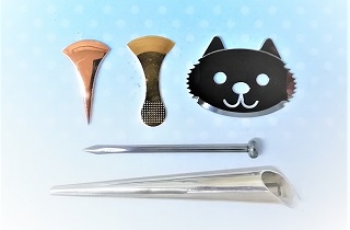
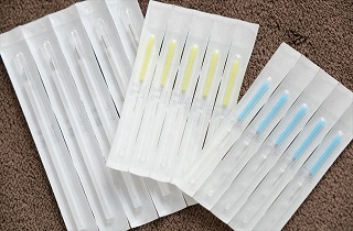
我们用的是一次性针灸针,所以每次都是用新的针灸针。
对于那些想要永远美丽的人。
全身调理完毕后,我们会治疗您担心的面部部位。刺激胶原蛋白的产生并增加紧致度和水分。它可以增强免疫系统并促进血液流动,帮助皮肤更新。
您不仅可以通过将针插入皮肤来感受效果,还可以通过用金属棒摩擦皮肤来感受效果。如果您有任何疑虑,请随时与我们联系。

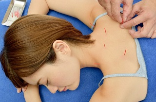
对于那些想要从广泛的肌肉疲劳中恢复过来的人。全身调好后,主要在背部进行拔罐。通过创造清洁血液和新鲜氧气的流动,抑制血液和气的停滞,改善身体障碍。
我们将主要治疗颈部和肩部。
全身治疗后,主要调整颈部和肩胛骨。舒缓肩膀僵硬、肩膀僵硬、颈部、肩部和背部的疼痛和紧张。
它还可以改善身体状况和偻引起的头痛。

我们将主要治疗腰部和臀部。
全身治疗后,主要调整腰部和骨盆。在日常生活中扭曲的骨骼结构和骨盆恢复到负担较小的状态。
它不仅可以缓解背部疼痛,还可以缓解膝盖疼痛。
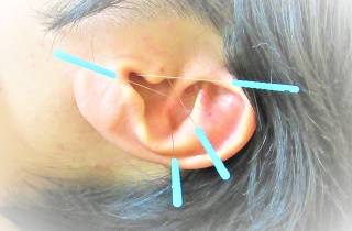
用耳穴调整全身。
全身治疗后,主要刺激耳穴。它会改善你的身体状况,让你更容易节食。除了针灸针,您还可以在首饰上贴上贴纸。珠宝几乎感觉不到疼痛。
对于因孩子的症状而烦恼的父母。
适用于小儿夜啼、疳虫、尿床等。
用金属刮刀轻轻擦拭皮肤。孩子们会觉得很舒服。
可以使用信用卡或二维码支付
我们接受 VISA、Mastercard、JCB、Amex、UnionPay、PayPay 等。
大塚针灸诊所的特点和 针灸治疗的机制

我们提供无痛且舒适的治疗,进而达到根治。我们擅长针灸,也擅长全身治疗。我们会告知您治疗计划,并就您的生活方式给您建议。

针灸不仅对肩酸背痛有效,而且对其他疾病的治疗也有疗效。它是国际公认的替代和补充医疗。世界卫生组织也对此列举了许多疾病病例和适应症清单。
针灸使用针灸针移动体内存在的气。它可以改善血液流动并增强自然治愈力。自然治愈力能缓解身体症状。
为了增强自然治愈力,针灸需要对有效的穴位进行刺激。针灸治疗的几千年的历史经验让我们掌握了关于穴位的知识。通过选择有效的穴位进行针灸,可以增强您的自然治愈力并改善您的症状。
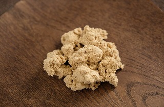
艾灸治疗相对缓慢,但效果持续时间长。艾灸能增强免疫力,促进血液流动。艾叶的气味具有镇静和治愈作用。对特定部位进行舒适的热刺激能缓解肌肉僵硬和双脚冰凉。改善经痛等女性特有的问题。

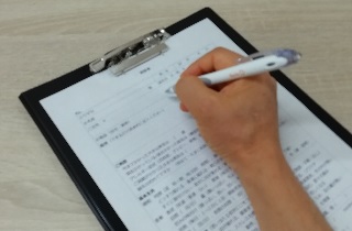
在本院进行的脉诊流经治疗中,我们采用四种诊断方法来掌握全身状况并找出症状的根本原因。通过对这一原因进行针灸治疗,我们的目标是改善或消除症状。
有四种诊断方法
・望诊:观察体色诊断
・闻诊:根据声音、音质、气味等进行诊断
・问诊:通过询问症状和生活习惯来诊断
・触诊:医师触摸患者的腹部和脉搏进行诊断
在东方医学中,没有四种诊断方法中的任何一种都不可能得出正确的诊断。我院在脉诊流经治疗中,特别注重触诊。我们可以从腹部的皮肤状况和脉搏的变化得知患者身体状况的变化,并预测症状好转的速度。
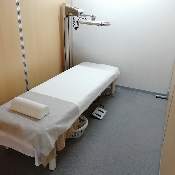
针灸治疗流程


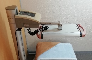
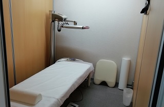
针灸诊所设备
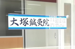
| 名称 | 大塚针灸诊所 |
| 地址 | 大阪府丰中市萤池中町3-8-14 |
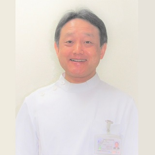
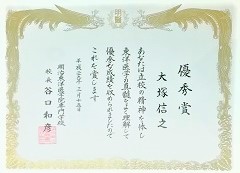
| 总监 | 大塚信之 |
| 访问 | 从阪急宝冢线和大阪单轨电车萤池站步行1分钟 |
| 停车位 | 针灸诊所右侧有 一个可停放一辆车的停车场 |
| 电话 | 代表+81-671669936, 直拨+81-8095319454 |
| 电子邮件 | otsuka.clinic* otsuka.holding.jp ※请用@替换* |
| 1962 | 出生于爱媛县东宇和郡宇和町鬼洼 |
| 1985 | 东北大学毕业 |
| 1987 | 东北大学研究生院 博士课程前期结业 加入松下电器,从事研发工作 |
| 1997 | 博士 (东北大学) 他被借调到通信放送机构 ,并与 西澤润一先生教授合着了很多书 |
| 1999 | 萤东洋医学研究所成立(代表) |
| 2017 | 明治东洋医学院专门学校毕业 获得针师执照和灸执照 明治东洋医学院专门学校临床实习生 开设大塚针灸诊所 东谷院(总监) |
| 2019 | 开设大塚针灸诊所 萤池院(总监) |
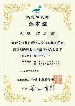
| 2022 | 全日本鍼灸学会 认定针灸师 |
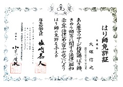
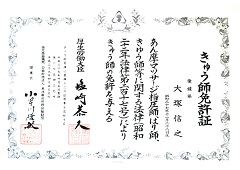
厚生劳动大臣执照
针师执照、灸师执照
东洋疗法学校协会 杰出表现奖
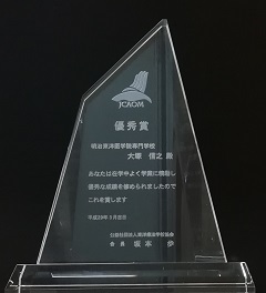
明治东洋医学院専门学校 杰出表现奖
●大塚信之. 针灸治疗失眠的应用. 萤东洋医学论文誌. Vol.9, No.1, pp.1-15, 2022.
●大塚信之. 针灸治疗耳鸣的应用. 萤东洋医学论文誌. Vol.8, No.1, pp.1-9, 2021.
●大塚信之. 针灸治疗痴呆早期发现.
萤东洋医学论文誌. Vol.7, No.1, pp.1-8, 2020.
●大塚信之, 半田由美子. 艾灸头针辐射光的点火位置依赖性和皮肤吸收特性.
全日本鍼灸学会杂誌. Vol.70, No.1,. Vol.70, No.1, pp.38-46, 2020.
●大塚信之. 针灸治疗双手麻木一例.
萤东洋医学论文誌. Vol.6, No.1, pp.1-6, 2019.
●大塚信之. 针灸在不孕不育中的应用.
萤东洋医学论文誌. Vol.5, No.1, pp.1-10, 2018.
●大塚信之. 针灸在糖尿病周围神经病变中的应用.
萤东洋医学论文誌. Vol.4, No.1, pp.1-9, 2017.
●大塚信之. 针灸在慢性疲劳综合征中的应用.
萤东洋医学论文誌. Vol.3, No.1, pp.1-9, 2016.
●大塚信之. 针灸的止痛作用.
萤东洋医学论文誌. Vol.2, No.1, pp.1-12, 2015.
●大塚信之. 针灸在运动损伤中的应用.
萤东洋医学论文誌. Vol.2, No.2, pp.1-13, 2015.
●大塚信之. 基于西医的女性疼痛与治疗方针.
萤东洋医学论文誌. Vol.1, No.1, pp.1-3, 2014.
●大塚信之. 针灸缓解痛经的疗效观察.
萤东洋医学论文誌. Vol.1, No.1, pp.4-6, 2014.
●大塚信之. 针灸对痴呆症的缓解作用.
萤东洋医学论文誌. Vol.1, No.2, pp.1-5, 2014.
●大塚信之. 针灸对下尿路功能障碍的影响.
萤东洋医学论文誌. Vol.1, No.3, pp.1-10, 2014.
●Nobuyuki Otsuka. Acupuncture and Moxibustion Treatment for Insomnia.
Hotal Traditional Oriental Medicine Letters Vol.9, No.1, pp.1-8, 2022.
●Nobuyuki Otsuka. Acupuncture and Moxibustion Treatment for Tinnitus.
Hotal Traditional Oriental Medicine Letters Vol.8, No.1, pp.1-6, 2021.
●Nobuyuki Otsuka. Acupuncture and Moxibustion Treatment for Early Detection of Dementia.
Hotal Traditional Oriental Medicine Letters Vol.7, No.1, pp.1-6, 2020.
●Nobuyuki Otsuka. Acupuncture and Moxibustion Treatment for Hands Numbness.
Hotal Traditional Oriental Medicine Letters Vol.6, No.1, pp.1-6, 2019.
●Nobuyuki Otsuka. Acupuncture and Moxibustion Treatment for Infertility.
Hotal Traditional Oriental Medicine Letters Vol.5, No.1, pp.1-6, 2018.
●Nobuyuki Otsuka. Acupuncture and Moxibustion Treatment for Diabetic Neuropathy.
Hotal Traditional Oriental Medicine Letters Vol.4, No.1, pp.1-4, 2017.
●Nobuyuki Otsuka. Acupuncture and Moxibustion Treatment for Chronic Fatigue Syndrome.
Hotal Traditional Oriental Medicine Letters Vol.3, No.1, pp.1-5, 2016.
●Nobuyuki Otsuka. Findings on Chronic Pain Management.
Hotal Traditional Oriental Medicine Letters Vol.2, No.1, pp.1-4, 2015.
●Nobuyuki Otsuka. Pain Relief Effect of Acupuncture and Moxibustion.
Hotal Traditional Oriental Medicine Letters Vol.2, No.1, pp.5-10,2015.
●Nobuyuki Otsuka. Acupuncture and Moxibustion Treatment for Sports Injurie.
Hotal Traditional Oriental Medicine Letters Vol.2, No.2, pp.1-5, 2015.
●Nobuyuki Otsuka. Pain of the Woman and Medical Treatment based on Western Medicine.
Hotal Traditional Oriental Medicine Letters Vol.1, No.1, pp.1-2, 2014.
●Nobuyuki Otsuka. Acupuncture Relieves Menstrual Pain.
Hotal Traditional Oriental Medicine Letters Vol.1, No.1, pp.3-4, 2014.
●Nobuyuki Otsuka. Acupuncture Relieves Dementing Disorder.
Hotal Traditional Oriental Medicine Letters Vol.1, No.2, pp.1-4, 2014.
●Nobuyuki Otsuka. Acupuncture and Moxibustion Treatment Relieves Lower Urinary Tract Dysfunction.
Hotal Traditional Oriental Medicine Letters Vol.1, No.3, pp.1-6, 2014.
学位论文
●大塚信之 金属有机气相外延法制备 InP 基半导体激光器的研究.
东北大学(2017).
GaN Power Diodes, GaN MMICs
●Toshihide Ide, Mitsuaki Shimizu, Xu Qiang Shen, Hidetoshi Ishida, Masahiro Ishida, Nobuyuki Otsuka, Tetsuzo Ueda. Recovery current characteristics of diode mode operation in GaN gate injection transistor bi-directional switch.
physica status solidi c, 14 (8) 1600245 (2017).
●Asamira Suzuki, Songbeak Choe, Yasuhiro Yamada, Nobuyuki Otsuka, Daisuke Ueda. NiO gate GaN-based enhancement-mode hetrojunction field-effect transistor with extremely low on-resistance using metal organic chemical vapor deposition regrown Ge-doped layer.
Jpn. J. Appl. Phys., 55, 121001 (2016).
●Toshihide Ide, Mitsuaki Shimizu, Xu Qiang Shen, Tatsuo Morita, Nobuyuki Otsuka, Tetsuzo Ueda. High accuracy equivalent circuit model for GaN GIT bi-directional switch.
physica status solidi c, 13 (5-6) 378-381 (2016).
●Shuichi Nagai, Yasuhiro Yamada, Noboru Negoro, Hiroyuki Handa, Miori Hiraiwa, Nobuyuki Otsuka, Daisuke Ueda. A 3-phase AC-AC matrix converter GaN chipset with drive-by-microwave technology.
IEEE Journal of the Electron Devices Society, 3 (1) 7-14 (2015).
●Toshihide Ide, Ryousaku Kaji, Mitsuaki Shimizu, Kenji Mizutani, Hiroaki Ueno, Nobuyuki Otsuka, Tetsuzo Ueda, Tsuyoshi Tanaka. Evaluation of radiated emission of GaN-HEMT switching circuit.
physica status solidi c, 11 (3-4) 936-939 (2014).
●S.Nagaia, Y.Yamadaa, Y. Kawaia, N. Negorob, H. Handab, M.Hiraiwaa, H.Uenoa, Y.Kudoha, K.Mizutania, M.Ishidab, T.Uedab, N.Otsuka, and D. Ueda. An Ultra Compact GaN 3x3 Matrix Converter.
ECS Transactions, 64 (7) 41-49 (2014).
●N. Otsuka, S. Nagai, M. Yanagihara, U. Uemoto and D. Ueda. Low-Pressure Direct-Liquid-Cooling Technology for GaN Power Transistors.
Jpn. J. Appl. Phys, Vol. 50 04DF07 (2011).
●N. Otsuka, S. Nagai, H. Ishida, Y. Uemoto T. Ueda, T. Tanaka, and D. Ueda. GaN Power Electron Devices.
ECS Transactions, 41 (8) 51-70 (2011).
GaN Blue Laser Diodes and Ultraviolet Light-Emitting Diodes
●K. Harafuji, Y. Hasegawa, A. Ishibashi, A. Tsujimura, N. Otsuka, I. Kidoguchi, and Y. Ban. Complex Flow and Gas Phase Chemical Reactions in GaN MOVPE Reactor.
Proc. Int. Workshop on Nitride Semiconductors, IPAP Conf.. Series 1 (2000) 101-104.
●A. Tsujimura, A. Ishibashi, Y. Hasegawa, S. Kamiyama, I. Kidoguchi, N. Otsuka, R. Miyanaga, G. Sugahara, M. Suzuki, M. Kume, K. Harafuji, and Y. Ban. Room-temperature CW operation of GaInN multiple quantum well laser diodes with optimized indium content.
Phys. Status Solidi A 176 (1999) 53-57.
●N. Otsuka, A. Tsujimura, Y. Hasegawa, G. Sugahara, M. Kume, and Y. Ban. 339 nm Deep-UV Emission from Al0.13Ga0.87N/Al0.10Ga0.90N Double Heterostructure Light-Emitting Diode on Sapphire Substrate.
Proc. Int. Workshop on Nitride Semiconductors, IPAP Conf.. Series 1 (2000) 837-840.
●N. Otsuka, A. Tsujimura, Y. Hasegawa, G. Sugahara, M. Kume, and Y. Ban. Room Temperature 339 nm Emission from Al0.13Ga0.87N/Al0.10Ga0.90N Double Heterostructure Light-Emitting Diode on Sapphire Substrate.
Jpn. J. Appl. Phys, 39 (2000) L445.
InP DFB lasers, InP strained MQW lasers
●N. Otsuka, M. Kito, Y. Yabuucni, M. Ishino, and Y. Matsui. Anomalous temperature dependence of PL characteristics in ordered InGaAsP strained layer multi-quantum well structure.
Journal of Crystal Growth 170 (1997) 626-633.
●M. Ishino, N. Takaneka, M. Kito, K. Fujihara, N. Otsuka, K. Fujito, and Y. Matsui. Low distortion 1.3 μm strained-layer MQW-DFB laser for AM-SCM transmission systems with large channel capacity.
J. Lightwave Technol. 15 (1997) 2172-2178.
●N. Otsuka, M. Kito, M. Ishino, and Y. Matsui. 1.5 μm strained-layer MQW-DFB lasers with high relaxation oscillation frequency and low chirp characteristics.
IEEE J. Quantum Electron 32 (1996) 1230-1236.
●N. Otsuka, M. Kito, Y. Yabuucni, M. Ishino, and Y. Matsui. Degradation of PL characteristics in strained layer multi-quantum well structure with atomic ordering structure.
Journal of Electronic Materials 25 (1996) 701-708.
●M. Kito, N. Otsuka, S. Nakamura, M. Ishino, and Y. Matsui. High-power, wide-temperature range operation of 1.3 μm gain-coupled DFB lasers with automatically buried InAsP absorptive grating.
IEEE Photon. Technol. Lett. 8 (1996) 1299-1301.
●M. Kito, S. Kimura, N. Otsuka, K. Fujihara, M. Ishino, and Y. Matsui. High output power operation of 1.3 μm strained MQW lasers with low threshold currents at high temperature.
Optical and Quantum Electron. 28 (1996) 503-511.
●M. Kito, S. Nakamura, N. Otsuka, M. Ishino and Y. Matsui. New structure of 1.3 μm strained-layer multi-quantum well complex-coupled distributed feedback lasers.
Jpn. J. Appl. Phys. 35 (1996) 1375-1377.
●M. Kito, N. Otsuka, M. Ishino, and Y. Matsui. Barrier composition dependence of differential gain and external differential quantum efficiency in 1.3-μm strained-layer multiquantum-well lasers.
IEEE J. Quantum Electron. 32 (1996) 38-42.
●竹中 直树, 鬼头 雅弘, 大塚 信之. 宽带SCM传输用畸变MQW-DFB激光模块.
National technical report 42(6) (1996) 708-713.
●M. Kito, H. Sato, N. Otsuka, N. Takenaka, M. Ishino, and Y. Matsui. Analysis of the second- and third-order intermodulation distortion in DFB lasers including dynamic spatial hole burning effect.
IEEE Photon. Technol. Lett. 7 (1995) 144-146.
●N. Otsuka, M. Kito, Y. Mori, M. Ishino, and Y. Matsui. New structure by selective regrowth in multi-quantum well laser diodes performed by low pressure metalorganic vapor phase epitaxy.
Journal of Crystal Growth 145 (1994) 866-874.
●M. Kito, N. Otsuka, M. Ishino, K. Fujihara, and Y. Matsui. Enhancement relaxation oscillation frequency of 1.3 μm strained-layer multiquantum well lasers.
IEEE Photon. Technol. Lett. 6 (1994) 690-693.
●M. Kito, M. Ishino, N. Otsuka, N. Hoshino, K. Fujihara, K. Fujito, and Y. Matsui. Low distortion up to 2 GHz in 1.55 μm multiquantum well distributed-feedback laser.
Electron. Lett. 28 (1992) 891-892.
Opto-Electronic Integrated circuit
●K. Matsuda, M. Kubo, N. Otsuka, and J. Shibata. Limitation factor of the bandwidth for InGaAs/InP monolithic photoreceiver.
J. Lightwave Technology 7 (1989) 2059-2063.
InP Molecular Layer Epitaxy
●N. Otsuka, J. Nishizawa, H. Kikuchi, and Y. Oyama. Expanded self-limiting growth condition of InP by alternate trimethylindium and tertiarybutylphosphine supply in ultrahigh vacuum.
J. Crystal Growth 209 (2000) 252-257.
●N. Otsuka, J. Nishizawa, H. Kikuchi, and Y. Oyama. Self-limiting Growth Conditions on (001) InP by Alternate Triethylindium and Tertiarybutylphosphine Supply in Ultrahigh Vacuum.
J. Vac. Sci. Technol. A17 (1999) 3008-3018.
●N. Otsuka, J. Nishizawa, H. Kikuchi, and Y. Oyama. Self-limiting growth of InP by alternate trimethylindium and tertiarybutylphosphine supply in ultrahigh vacuum.
J. Crystal Growth 205 (1999) 253-263.
●N. Otsuka, J. Nishizawa, H. Kikuchi, and Y. Oyama. Self-limiting submonolayer growth of InP by alternative triethylindium and tertiarybutylphosphine supply in ultra high vacuum.
Inst. Phys. Conf. Ser 162 (1999) 529-534.
●N. Otsuka, J. Nishizawa, H. Kikuchi, and Y. Oyama. Self-Limiting Growth of Specular InP Layer by Alternate Injection of Triethylindium and Tertiarybutylphosphine in Ultrahigh Vacuum.
Jpn. J. Appl Phys. 38 (1999) L20-L23.
InP Self-limiting Etching
●N. Otsuka, J. Nishizawa, Y. Oyama, H. Kikuchi, and K. Suto. Self-limiting etching prior to self-limiting growth in ultra-high vacuum for obtaining clean interface.
International Conference for The Physics of Semiconductors (2001) .
●N. Otsuka, J. Nishizawa, Y. Oyama, H. Kikuchi, and K. Suto. Digital Etching of InP by Intermittent Injection of Phosphorous Precursors in Ultra-high Vacuum.
Jpn. J. Appl Phys. 38 (1999) 2529-2537.
●N. Otsuka, J. Nishizawa, Y. Oyama, H. Kikuchi, and K. Suto. Digital etching of InP by intermittent injection of tris-dimethylaminophosphorus in ultra high vacuum.
J. Electrochem. Soc.. 146 (1999) 547-550.
●N. Otsuka, Y. Oyama, H. Kikuchi, J. Nishizawa, and K. Suto. Digital etching of (001) InP substrate by intermittent injection of tertiarybutylphosphine in ultrahigh vacuum.
Jpn. J. Appl Phys. 37 (1998) L1509-L1512.
InP MOVPE growth
●N. Otsuka, M. Ishino, and Y. Matsui, F. Toujou. Control of double diffusion front unintentionally penetrated from a Zn doped InP layer during metalorganic vapor phase epitaxy.
J. Appl. Phys. 84 (1998) 4239-4247.
●N. Otsuka, M. Ishino, and Y. Matsui. Stability of Zn doping profile in modulation doped multiple quantum well structure.
J. Appl. Phys. 80 (1996) 1405-1413.
●M. Shiojiri, T. Isshiki, K. Nishino, M. Tsujikura, J. Saijo, Y. Takahashi, N. Ohtsuka, and Y. Yabuuchi. Quantitative Structure Images of Interfaces in InGaAs/InP Multilayer Heterostructures.
J. Electron Microsc 41 (1992) 434-444. and Ultramicroscopy.
●Y. Yabuuchi, Y. Takahashi, N. Ohtsuka, T. Isshiki, M. Tsujikura, H. Saijo, and M. Shiojiri. High-Resolution Transmission Electron Microscopy Observations of InGaAs/InP Multilayer Heterostructures.
Phys. Stat. Sol. (a) 127 (1991) 385-396.
Mg2Si1-xGex compound semiconductors
●Y. Noda, H. Kon, Y. Furukawa, N. Otsuka, I. Nishida, and K. Masumoto. Preparation and thermoelectric properties of Mg2Si1-xGex (x=0.0~0.4) solid solution semiconductors.
Materials Transactions, JIM 33 (1992) 845-850.
●Y. Noda, N. Otsuka, K. Masumoto, and I. Nishida. Preparation of thermoelectric properties of Mg2Si1-xGex solid-solution semiconductor.
Nippon Kinzoku Gakkai-si 53(5) (1989) 487-493.
●大塚信之, 半田由美子. 通过体重的时间序列分析来检验针灸治疗的效果.
第71次 全日本鍼灸学会学术大会2022 摘要书 No.037. pp.162, 2022.
●大塚信之, 半田由美子. 知热灸的燃烧特性及热效应对灸高的依赖性.
第70次 全日本鍼灸学会学术大会2021 摘要书 No.005. pp.128, 2021.
●大塚信之. 中隔灸的燃烧特性及热效应对灸形的依赖性.
全日本鍼灸学会杂誌. Vol.70, No.3, pp.156, 2020.
●大塚信之, 半田由美子. 艾灸头针辐射光的皮肤吸收特性.
第68次 全日本鍼灸学会学术大会2019 摘要书 No.217 2-P-I(4). pp.236, 2019.
●大塚信之. 针灸治疗腹股沟疝有效一例.
第67次 全日本鍼灸学会学术大会2018 摘要书 No.129 2-P-E1(2). pp.224, 2018.
GaN Power devices, GaN MMICs
●D. Ueda, M. Hikita, S. Nakazawa, K. Nakazawa, H. Ishida, M. Yanagihara, K. Inoue, T. Ueda, Y. Uemoto, T. Tanaka, N. Otsuka and Takashi Egawa, " GaN-Based Power Devices", in Tech Digest of International Symposium on Advanced Nanodevices and Nanotechnology 2009 (ISANN2009) (Kaanapali, Maui, Hawaii, USA, November 29-December 4, 2009).
●N. Otsuka, S. Nagai, M. Yanagihara, U. Uemoto and D. Ueda " Direct Liquid Cooling Technology for Power Semiconductor Devices " in Extended Abstracts of the 2010 International Conference on Solid State Devices and Materials, Tokyo, 2010, pp1229-1230.
●(Invited) N. Otsuka, S. Nagai, H. Ishida, Y. Uemoto T. Ueda, T. Tanaka, and D. Ueda "GaN Power Electron Devices" in Extended Abstracts of the 220th ECS Meeting, Electrochemical Society, Boston, 2011, Abstract #2170.
●K. Mizutani, H. Ueno, Y. Kudoh, S. Nagai, K. Inoue, N. Otsuka, T. Ueda, T. Tanaka and D. Ueda "Integrated Power Design Platform based on Modeling Dynamic Behavior of GaN Devices, in Technical Digest of the IEDM 2011, 2011 IEEE International Electron Devices Meeting, Washington, DC, 2011, 26.4.1.
●S. Nagai, T. Kojima, M. Koyama, T. Shiraishi, Y. Kudoh, N. Otsuka, A. Ikoshi, Y. Uemoto, T. Ueda, T. Tanaka, K. Inoue and D. Ueda " An Ultra Compact Dual-Side Cooled Surface Mount GaN Multi-chip Inverter Package with Cu Leads Direct Bonding" in Abstract of the 9th Topical Workshop on Heterostructure Microelectronics , TWHM 2011, Gifu, 2011, 103.
●(Invited) K. Mizutani, H. Ueno, Y. Kudoh, S. Nagai, K. Inoue, N. Otsuka, T. Ueda, T. Tanaka and D. Ueda "Integrated Power Design Platform for Power Electronics Applications with GaN Devices" in Workshop Digest of the AWAD 2012, 2012 Asia-Pacific Workshop on Fundamentals and Applications of Advanced Semiconductor Devices, Okinawa, 2012, 302.
●R. Baert, M. Badaroglu, K. Mizutani, H. Ueno, Y. Kudoh, S. Nagai, K. Inoue, N. Otsuka, and D. Ueda "Fast Simulation of Power Electronic Systems by Partitioning, Segmentation and Caching" in Abstract of 13th IEEE Workshop on Control and Modeling for Power Electronics, COMPEL'12, 2012, Kyoto.
●(Invited) N. Otsuka, "GaN Power Electron Devices" International SiC Power Electronics Applications Workshop, ISiCPEAW2012, Stockholm, 2012.
●S. Nagai, N. Negoro, T. Fukuda, H. Sakai, T. Ueda, T. Tanaka, N. Otsuka and D. Ueda "Drive-by-Microwave Technologies for Isolated Direct Gate Drivers" in Proceeding of 2012 IEEE MTT-S International Microwave Workshop Series (IMWS) on Innovative Wireless Power Transmission: Technologies, Systems, and Applications, IMWS-IWPT2012, Kyoto, 2012, 267-270.
●S. Nagai, N. Negoro, T. Fukuda, N. Otsuka, H. Sakai, T. Ueda, T. Tanaka and D. Ueda "A DC-Isolated Gate Drive IC With Drive-by-Microwave Technology for Power Switching Devices" in Proceeding of 2012 IEEE International Solid-State Circuits Conference, ISSCC 2012, San Francisco, 2012, 404-406.
●S. Nagai, T. Fukuda, N. Otsuka, D. Ueda , N. Negoro, H. Sakai, T. Ueda, T. Tanaka "A One-chip Isolated Gate Drive with an Electromagnetic Resonance Coupler Using a SPDT switch" in Proceeding of the 2012 24th International Symposium on Power Semiconductor Devices and ICs, ISPSD 2012, Bruges, 2012, 73-76.
●(Invited) D. Ueda , N. Otsuka, S. Nagai, N. Negoro, T. Fukuda, H. Sakai, T. Morita, T. Ueda, T. Tanaka "A Novel Insulated GaN Gate-Driver with Wireless Power Transfer Technology", in abstract of the International Workshop on Nitride Semiconductors 2012, IWN2012, Sapporo, 2012,
●(Invited) N. Otsuka, " Recent Progress on GaN-based Power Devices " International Workshop on Wide-Band-Gap Power Electronics 2013, IWWPE2013, Hsinchu, 2013.
●A. Suzuki, Y. Yamada, H. Tanaka, H. Ueno, N. Otsuka, Y. Anda, T. Ueda, T. Tanaka, and D. Ueda, "Low on-state resistance normally-off AlGaN/GaN HFET with ALD formed p-type NiO Gate", in proceedings of the 37th workshop on compound semiconductor devices and integrated cirquits, WOCSDICE 2013, Warnemunde, 2013.
●Toshihide Ide, Ryousaku Kaji, Mitsuaki Shimizu, Kenji Mizitani, Hiroaki Ueno, Nobuyuki Otsuka , Tetsuzo Ucda and Tsuyoshi Tanaka "Evaluation of Radiated Emission of GaN-HEMT Switching Circuit.", in abstract of 10th International Conference on Nitride Semiconductors 2013, ICNS-10, Washington, D.C., 2013, 31, DP3.08
●(Invited) N. Otsuka, " Recent Progress in GaN Power Devices " The 6th International Symposium on Advanced Plasma Science and its Applications for Nitrides and Nanomaterials, ISPlasma2014, Nagoya, 2014.
●Yuji Kudoh, Nobuyuki Otsuka, Kenji Mizutani, Toshimitsu Morizane “A Novel Single to Two-Phase Matrix Converter for Driving A Symmetrically Designed Two-Phase Induction Motor”, IEEE 10th International Conference on Power Electronics and Drive Systems (PEDS), 2013, April, 1133-1138.
●S. Nagai, Y. Yamada, N. Negoro, H. Handa, Y. Kudoh, H. Ueno, M. Ishida, N. Otuska, D. Ueda ” A GaN 3×3 Matrix Converter Chipset with Drive-by-Microwave Technologies” 2014 IEEE International Solid-State Circuits Conference, 30.5
●Yuji Kudoh, Kenji Mizutani, Nobuyuki Otsuka, Satoru Takahashi, Masahiko, Inamori, Hiroto Yamagiwa, Tatsuo Morita, Tetsuzo Ueda, Tsuyoshi Tanaka, Daisuke Ueda, Toshimitsu Morizane, “Single to 2-phase Matrix Converter using GaN-based Monolithic Bidirectional Switch for Driving Symmetrical 2-phase Motor” IEEE Energy Conversion Congress and Exhibition (ECCE 2014) P7103.
●A. Suzuki, S. Choe, Y. Yamada, S. Nagai, M. Hiraiwa, N. Otsuka. D. Ueda “Extremely low on-resistance enhancement-mode GaN-based HFET using Ge-doped regrowth technique”, Electron Devices Meeting, IEDM (2014).
●Tetsuya Yamamoto; Tetsuro Sawai; Kenji Mizutani; Nobuyuki Otsuka; Eiji Fujii; Nobuyuki Horikawa; Yoshihiko Kanzawa, “A novel duality-based modeling methodology for reverse current-voltage characteristics of SiC”, 2014 International Conference on Simulation of Semiconductor Processes and Devices (SISPAD), pp. 53-55 (2014).
●Daisuke Ueda; Takeshi Fukuda; Shuichi Nagai; Hiroyuki Sakai; Nobuyuki Otsuka; Tatsuo Morita; Noboru Negoro; Tetsuzo Ueda; Tsuyoshi Tanaka, “Present and Future of GaN Power Devices”, CIPS 2014; 8th International Conference on Integrated Power Electronics Systems, pp. 1-5 (2014).
●Shuichi Nagai; Yasufumi Kawai; Osamu Tabata; Hideaki Fujiwara; Nobuyuki Otsuka; Daisuke Ueda; Noboru Negoro; Masahiro Ishida, “A compact Drive-by-Microwave gate driver with coupler integrated in a package”, 2014 IEEE Applied Power Electronics Conference and Exposition - APEC 2014, pp. 1461 - 1464 (2014).
●Shuichi Nagai; Yasufumi Kawai; Osamu Tabata; Hideaki Fujiwara; Noboru Negoro; Masahiro Ishida; Nobuyuki Otsuka, “A Drive-by-Microwave isolated gate driver with gate current charge for IGBTs”, 2014 16th European Conference on Power Electronics and Applications, pp. 1 - 6 (2014).
●Shuichi Nagai; Yasufumi Kawai; Osamu Tabata; Hideaki Fujiwara; Yasuhiro Yamada; Nobuyuki Otsuka; Daisuke Ueda; Noboru Negoro; Masahiro Ishida, “A Drive-by-Microwave isolated gate driver with a high-speed voltage monitoring”, 2014 IEEE 26th International Symposium on Power Semiconductor Devices & IC's (ISPSD) 434-437 (2014).
●Yasufumi Kawai; Shuichi Nagai; Osamu Tabata; Hideaki Fujiwara; Noboru Negoro; Hiroaki Ueno; Masahiro Ishida; Nobuyuki Otsuka “An isolated DC power supply free compact GaN inverter module”, 2015 IEEE 11th International Conference on Power Electronics and Drive Systems, pp. 84-88 (2015).
●(Invited) Nobuyuki Otsuka; Yasufumi Kawai; Shuichi Nagai “Recent progress in GaN devices for power and integrated circuit”, 2017 IEEE 12th International Conference on ASIC (ASICON), pp. 928 - 931 (2017).
GaN Blue Laser Diodes and Ultraviolet Light-Emitting Diodes
●N. Otsuka, A. Tsujimura, Y. Hasegawa, G. Sugahara, M. Kume, and Y. Ban “339 nm Deep-UV Emission from Al0.13Ga0.87N/Al0.10Ga0.90N Double Heterostructure Light-Emitting Diode on Sapphire Substrate”, in Tech Digest of International Workshop on Nitride Semiconductors (IWN2000) (Nagoya, Japan, 2000) paper WM1-2, pp. 114.
●K. Harafuji, Y. Hasegawa, A. Ishibashi, A. Tsujimura, N. Otsuka, I. Kidoguchi, and Y. Ban “Complex Flow and Gas Phase Chemical Reactions in GaN MOVPE Reactor”, in Tech Digest of International Workshop on Nitride Semiconductors (IWN2000) (Nagoya, Japan, 2000) paper PMD-22, pp. 172.
InP DFB lasers, InP strained MQW lasers
●N. Otsuka, M. Ishino, M. Kito, K. Hoshino, K. Fujihara, K. Fujito, and Y. Matsui, "Low distortion over wide-band modulation of 1.55-?m MQW distributed-feedback lasers", in Tech Digest of Optical Fiber Communication Conference '92 (San Jose, California, 1992) Paper FB5, pp. 275.
●N. Otsuka, M. Ishino, K. Fujihara, M. Kito, Y. Mori, H. Sato, and Y. Matsui, "Low-chirp characteristics over wide-band modulation of multiple-quantum-well distributed-feedback lasers", in Tech Digest of 9th International Conference on Integrated Optics and Optical Fiber Communication '93 (San Jose, California, 1993) Paper WH15, pp. 127-128.
●N. Otsuka, M. Kito, Y. Mori, M. Ishino, and Y. Matsui, "New structure by selective regrowth in MQW laser diodes performed by low pressure MOVPE", in Proc. 7th International Conference on Metalorganic Vapor Phase Epitaxy (Yokohama, Japan, 1994) Paper P3-2, pp. 268-269.
●N. Otsuka, M. Kito, Y. Yabuucni, M. Ishino, and Y. Matsui, "Atomic ordering in strained layer multi-quantum well structure", in Proc. 7th International Conference on Indium Phosphide and Related Materials (Sapporo, Japan, 1995) Paper FA1.4, pp. 701-704.
●N. Otsuka, M. Kito, M. Ishino, and Y. Matsui, "1.5 ?m strained-layer MQW-DFB lasers with low chirp and low distortion characteristics", in Tech Digest of 10th International Conference on Integrated Optics and Optical Fiber Communication '95 (Hong Kong, 1995) Paper FB2-6, pp. 50-51.
●N. Otsuka, M. Kito, Y. Yabuucni, M. Ishino, and Y. Matsui, "Anomalous temperature dependence of PL characteristics in ordered InGaAsP strained layer multi-quantum well structure", in Proc. 8th International Conference on Metalorganic Vapor Phase Epitaxy (Weales, England, 1996) Paper OSSP.6.
●M. Ishino, K. Fujihara, N. Otsuka, N. Takenaka, T. Uno, and Y. Matsui, “High performance analog transmission characteristics of 1.3 ?m wavelength multiquantum well distributed feedback laser,” in Tech Digest of Optical Fiber Communication Conference '91 (San Diego, California, 1991) Paper WG6, pp. 93.
●M. Kito, N. Otsuka, K. Fujihara, S. Yamane, M. Ishino, K. Fujito, and Y. Matsui, “Extremely low bias current operation of 1.3 ?m strained-layer MQW-DFB laser for 97 ch AM-FDM transmission,” in Extended Abstract 1993 International Conference Solid State Devices and Materials (Chiba, Japan,1993) Paper D-6-4, pp. 1035-1037.
●K. Fujihara, Y. Mori, M. Kito, N. Otsuka, M. Ishino, and Y. Matsui, “High characteristics temperature 1.48?m strained-layer MQW laser diode with wide bandgap barrier layers,” IEDM ‘93 (Wasnington, D.C., 1993) Paper 23.5, pp. 605-608.
●M. Ishino, M. Kito, S. Yamane, K. Fujihara, N. Otsuka, H. Sato, and Y. Matsui, “1.3 ?m strained-layer MQW-DFB laser with low noise and low distortion characteristics for 100-channel CATV transmission,” in Tech Digest of International Electron Devices Meeting 1993 (Washington, DC., 1993) Paper 23.7, pp. 613-616.
●M. Kito, H. Sato, N. Otsuka, N. Takenaka, M. Ishino and Y. Matsui, “The effect of dynamic spatial hole burning on the second and third order intermodulation distortion in DFB lasers,”in Proc. 14th IEEE Int. Semiconductor Laser Conf. (Maui, Hawaii, 1994) Paper T2.6, pp. 57-58.
●M. Kito, H. Sakai, N. Otsuka, K. Fujihara, M. Ishino and Y. Matsui, “High output power operation of 1.3 ?m strained MQW lasers with low threshold currents at high temperature,” in Proc. 7th International Conference on Indium Phosphide and Related Materials (Sapporo, Japan, 1995) Paper ThP37, pp. 508-511.
●M. Kito, S. Nakamura, N. Otsuka, M. Ishino and Y. Matsui, “Novel structure of 1.3 ?m strained-layer MQW complex-coupled DFB lasers,” in Extended Abstract 1995 International Conference Solid State Devices and Materials (Osaka, Japan, 1995) Paper D-4-3, pp. 431-433.
●M. Kito, N. Otsuka, S. Nakamura, M. Ishino and Y. Matsui, “High-power, wide-temperature range operation of 1.3-?m complex-coupled DFB lasers with automatically buried absorptive grating,” in Tech Digest of Optical Fiber Communication ‘96, (San Jose, California, 1996) Paper TuH5, pp. 38-39.
●J. Ohya, N. Otsuka, S. Nakamura, Y. Inaba, M. Ishino, Y. Matsui, M. Fuse, K. Nojima, Y. Ishii, S. Kawashima, and S, Kitaji, “Low noise and low distortion AM/FM converter with frequency modulated 1.55?m strained-layer MQW-DFB laser for analog transmission,” in Tech Digest of 11th international conference on Integrated Optics and Optical Fiber Communications/23rd European Conference on Optical Communications, (Edinburgh, UK, 1997) pp. 94-97.
Opto-Electronic Integrated circuit
●N. Otsuka, K. Matsuda, and J. Shibata, "InGaAs/InP Monolithic Array Photoreceiver Consisting of 10 PIN/FET's", in Tech Digest of 7th International Conference on Integrated Optics and Optical Fiber Communication '89 (Kobe, Japan, 1989) Paper 20C4-1, pp. 166-167.
InP Molecular Layer Epitaxy
●N. Otsuka, J. Nishizawa, H. Kikuchi, and Y. Oyama, “Self-limiting submonolayer growth of InP by alternative triethylindium and tertiarybutylphosphine supply in ultra high vacuum,” in Tech Digest of 25th International Symposium on Compound Semiconductors (ISCS'98), (Nara, Japan, 0998) paper TuP-2.
●N. Otsuka, J. Nishizawa, H. Kikuchi, and Y. Oyama, “Extended self-limiting growth condition of InP using alternate trimethylindium and tertiarybutylphosphine supply in ultrahigh vacuum,” in Tech Digest of 7th International Conference on Chemical Beam Epitaxy and Related Growth Techniques (ICCBE’99), (Tsukuba, Japan, 1999) paper We3-8.
InP Self-limiting Etching
●N. Otsuka, J. Nishizawa, Y. Oyama, H. Kikuchi, and K. Suto, “Digital etching of InP using tris-dimethylaminophosphorus in ultra-high vacuum,” in Tech Digest of 1998 International Conference on Solid-State Devices and Materials (SSDM'98), (Hiroshima, Japan, 1998) paper D-4-6, pp.238.
●N. Otsuka, J. Nishizawa, Y. Oyama, H. Kikuchi, and K. Suto, “Self-limiting etching prior to self-limiting growth in ultra-high vacuum for obtaining clean interface,” in Tech Digest of 25th International Conference for The Physics of Semiconductors (ICPS25), (Osaka, Japan, 2000) paper D052.
InP MOVPE growth
●Y. Yabuuchi, Y. Takahashi, N. Otsuka, T. Isshiki, K. Nishio, M. Tsujikura, H. Saijo, and M. Shiojiri, “HRTEM of heterointerfaces in InGaAs/InP multilayer crystals,” in proc. 5th Asia-Pacific Electron Microscopy Conference (Beijin, China, 1992) pp. 572-573.
●Y. Yabuuchi, Y. Takahashi, N. Otsuka, T. Isshiki, K. Nishio, M. Tsujikura, H. Saijo, and M. Shiojiri, “HRTEM images of InGaAs/InP multilayer heterostructures,” in proc. 10th European Congress on Electron Microscopy (Gramada, Spain, 1992) pp. 167-168.
●Nobuyuki Otsuka. Modern kana notation Shinkyu-tyouhouki-koumoku. 蛍東洋医学研究所 (2022).
●Nobuyuki Otsuka. Translated by Hotal Ancient Medicine Research Institute Shindou-hiketsu-syu. 蛍東洋医学研究所 (2021).
●Nobuyuki Otsuka, Shuichi Nagai, Daisuke Ueda. Power Device Packaging Technology, Chapter 4. Science & Technology, 239-262 (2012).