HOME > ごあいさつのページ
[HARI] Hotal Traditional Oriental Medicine

お問い合わせをお待ちしております
TEL.06-7166-9936
営業時間 AM9:00 ~ PM20:00

ごあいさつ

東洋医学に関する基礎的内容から最近の研究発表についてご紹介します。

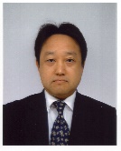
代表 大塚 信之

代表 大塚 信之


経 歴

漢方、鍼灸、気功など、東洋医学に関する研究に従事

 昭和37年 愛媛県東宇和郡宇和町鬼窪に生誕
 昭和60年 東北大学 卒業
 昭和62年 東北大学 大学院前期博士課程 修了
松下電器産業(株)入社 研究開発に従事
 平成 9年 博士(東北大学)
通信放送機構 西澤潤一先生との共著多数
 平成11年 蛍東洋医学研究所 設立
 平成29年 明治東洋医学院専門学校 卒業
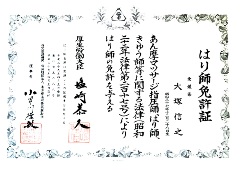
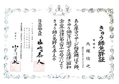
はり師、きゅう師免許 取得
明治東洋医学院専門学校治療所 卒後臨床研修生
大塚鍼灸院 東谷院 開設
 平成31年 大塚鍼灸院 蛍池院 開設
 令和 3年 パナソニック(株)定年扱退職
鍼灸治療に専念
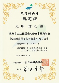
 令和 4年 全日本鍼灸学会 認定鍼灸師


資格・表彰・研究業績

リサーチマップからもご確認いただけます

資格・認定

厚生労働大臣免許証
はり師免許証、きゅう師免許証
はり師免許証 きゅう師免許証


全日本鍼灸学会 認定鍼灸師
全日本鍼灸学会認定鍼灸師

表彰

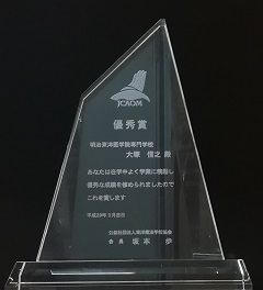
東洋療法学校協会 優秀賞 平成29年3月
東洋療法学校協会優秀賞

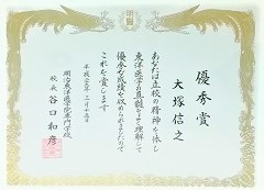
明治東洋医学院専門学校 優秀賞 平成29年3月
明治東洋医学院専門学校優秀賞

優秀特待生 明治東洋医学院専門学校 平成28年4月26日


IEEE EDS Kansai Chapter IMFEDK Best Paper Award 2013


研究業績


所属学術団体


所属鍼灸専門団体


お問い合わせ

蛍東洋医学研究所
[HARI] Hotal Ancient Medicine Research Institute
for Acupuncture and Moxibustion Research

icon 電話番号06-7166-9936
ご不明な点がございましたら、まずはお気軽にご相談下さい。
→メールでのお問い合わせ


ページトップに戻る


論文

東洋医学分野

●Nobuyuki Otsuka. Acupuncture and Moxibustion Treatment for Insomnia. Hotal Traditional Oriental Medicine Letters Vol.9, No.1, pp.1-8, 2022.
●大塚信之. 不眠症への鍼灸の適用. 蛍東洋医学論文誌. Vol.9, No.1, pp.1-15, 2022.
●Nobuyuki Otsuka. Acupuncture and Moxibustion Treatment for Tinnitus. Hotal Traditional Oriental Medicine Letters Vol.8, No.1, pp.1-6, 2021.
●大塚信之. 耳鳴への鍼灸の適用. 蛍東洋医学論文誌. Vol.8, No.1, pp.1-9, 2021.
●Nobuyuki Otsuka. Acupuncture and Moxibustion Treatment for Early Detection of Dementia. Hotal Traditional Oriental Medicine Letters Vol.7, No.1, pp.1-6, 2020.
●大塚信之. 認知症の早期検知に向けた鍼灸治療. 蛍東洋医学論文誌. Vol.7, No.1, pp.1-8, 2020.
●大塚信之, 半田由美子. 灸頭鍼から輻射される光の点火位置依存性と皮膚吸収特性. 全日本鍼灸学会雑誌. Vol.70, No.1, pp.38-46, 2020.
●Nobuyuki Otsuka. Acupuncture and Moxibustion Treatment for Hands Numbness. Hotal Traditional Oriental Medicine Letters Vol.6, No.1, pp.1-6, 2019.
●大塚信之. 両手のしびれに対して鍼灸治療を適用した一症例. 蛍東洋医学論文誌. Vol.6, No.1, pp.1-6, 2019.
●Nobuyuki Otsuka. Acupuncture and Moxibustion Treatment for Infertility. Hotal Traditional Oriental Medicine Letters Vol.5, No.1, pp.1-6, 2018.
●大塚信之. 不妊症への鍼灸の適用. 蛍東洋医学論文誌. Vol.5, No.1, pp.1-10, 2018.
●Nobuyuki Otsuka. Acupuncture and Moxibustion Treatment for Diabetic Neuropathy. Hotal Traditional Oriental Medicine Letters Vol.4, No.1, pp.1-4, 2017.
●大塚信之. 糖尿病性末梢神経障害への鍼灸の適用. 蛍東洋医学論文誌. Vol.4, No.1, pp.1-9, 2017.
●Nobuyuki Otsuka. Acupuncture and Moxibustion Treatment for Chronic Fatigue Syndrome. Hotal Traditional Oriental Medicine Letters Vol.3, No.1, pp.1-5, 2016.
●大塚信之. 慢性疲労症候群への鍼灸の適用. 蛍東洋医学論文誌. Vol.3, No.1, pp.1-9, 2016.
●Nobuyuki Otsuka. Findings on Chronic Pain Management. Hotal Traditional Oriental Medicine Letters Vol.2, No.1, pp.1-4, 2015.
●Nobuyuki Otsuka. Pain Relief Effect of Acupuncture and Moxibustion. Hotal Traditional Oriental Medicine Letters Vol.2, No.1, pp.5-10,2015.
●Nobuyuki Otsuka. Acupuncture and Moxibustion Treatment for Sports Injurie. Hotal Traditional Oriental Medicine Letters Vol.2, No.2, pp.1-5, 2015.
●大塚信之. 鍼灸治療による疼痛緩和効果. 蛍東洋医学論文誌. Vol.2, No.1, pp.1-12, 2015.
●大塚信之. スポーツ傷害への鍼灸の適用. 蛍東洋医学論文誌. Vol.2, No.2, pp.1-13, 2015.
●Nobuyuki Otsuka. Pain of the Woman and Medical Treatment based on Western Medicine. Hotal Traditional Oriental Medicine Letters Vol.1, No.1, pp.1-2, 2014.
●Nobuyuki Otsuka. Acupuncture Relieves Menstrual Pain. Hotal Traditional Oriental Medicine Letters Vol.1, No.1, pp.3-4, 2014.
●Nobuyuki Otsuka. Acupuncture Relieves Dementing Disorder. Hotal Traditional Oriental Medicine Letters Vol.1, No.2, pp.1-4, 2014.
●Nobuyuki Otsuka. Acupuncture and Moxibustion Treatment Relieves Lower Urinary Tract Dysfunction. Hotal Traditional Oriental Medicine Letters Vol.1, No.3, pp.1-6, 2014.
●大塚信之. 西洋医学に基づいた女性の痛みと治療方針. 蛍東洋医学論文誌. Vol.1, No.1, pp.1-3, 2014.
●大塚信之. 鍼灸による月経痛の緩和効果. 蛍東洋医学論文誌. Vol.1, No.1, pp.4-6, 2014.
●大塚信之. 認知症疾患に及ぼす鍼治療の緩和効果. 蛍東洋医学論文誌. Vol.1, No.2, pp.1-5, 2014.
●大塚信之. 下部尿路機能障害に対する鍼灸治療の効果. 蛍東洋医学論文誌. Vol.1, No.3, pp.1-10, 2014.

元に戻る


論文

電気電子分野

学位論文
●大塚信之. 有機金属気相成長法によるInP系半導体レーザの作製に関する研究. 東北大学 学位論文(博士)(2017).

GaN Power Diodes, GaN MMICs
●Toshihide Ide, Mitsuaki Shimizu, Xu Qiang Shen, Hidetoshi Ishida, Masahiro Ishida, Nobuyuki Otsuka, Tetsuzo Ueda. Recovery current characteristics of diode mode operation in GaN gate injection transistor bi-directional switch. physica status solidi c, 14 (8) 1600245 (2017).
●Asamira Suzuki, Songbeak Choe, Yasuhiro Yamada, Nobuyuki Otsuka, Daisuke Ueda. NiO gate GaN-based enhancement-mode hetrojunction field-effect transistor with extremely low on-resistance using metal organic chemical vapor deposition regrown Ge-doped layer. Jpn. J. Appl. Phys., 55, 121001 (2016).
●Toshihide Ide, Mitsuaki Shimizu, Xu Qiang Shen, Tatsuo Morita, Nobuyuki Otsuka, Tetsuzo Ueda. High accuracy equivalent circuit model for GaN GIT bi-directional switch. physica status solidi c, 13 (5-6) 378-381 (2016).
●Shuichi Nagai, Yasuhiro Yamada, Noboru Negoro, Hiroyuki Handa, Miori Hiraiwa, Nobuyuki Otsuka, Daisuke Ueda. A 3-phase AC-AC matrix converter GaN chipset with drive-by-microwave technology. IEEE Journal of the Electron Devices Society, 3 (1) 7-14 (2015).
●Toshihide Ide, Ryousaku Kaji, Mitsuaki Shimizu, Kenji Mizutani, Hiroaki Ueno, Nobuyuki Otsuka, Tetsuzo Ueda, Tsuyoshi Tanaka. Evaluation of radiated emission of GaN-HEMT switching circuit. physica status solidi c, 11 (3-4) 936-939 (2014).
●S.Nagaia, Y.Yamadaa, Y. Kawaia, N. Negorob, H. Handab, M.Hiraiwaa, H.Uenoa, Y.Kudoha, K.Mizutania, M.Ishidab, T.Uedab, N.Otsuka, and D. Ueda. An Ultra Compact GaN 3x3 Matrix Converter. ECS Transactions, 64 (7) 41-49 (2014).
●N. Otsuka, S. Nagai, M. Yanagihara, U. Uemoto and D. Ueda. Low-Pressure Direct-Liquid-Cooling Technology for GaN Power Transistors. Jpn. J. Appl. Phys, Vol. 50 04DF07 (2011).
●N. Otsuka, S. Nagai, H. Ishida, Y. Uemoto T. Ueda, T. Tanaka, and D. Ueda. GaN Power Electron Devices. ECS Transactions, 41 (8) 51-70 (2011).

GaN Blue Laser Diodes and Ultraviolet Light-Emitting Diodes
●K. Harafuji, Y. Hasegawa, A. Ishibashi, A. Tsujimura, N. Otsuka, I. Kidoguchi, and Y. Ban. Complex Flow and Gas Phase Chemical Reactions in GaN MOVPE Reactor. Proc. Int. Workshop on Nitride Semiconductors, IPAP Conf.. Series 1 (2000) 101-104.
●A. Tsujimura, A. Ishibashi, Y. Hasegawa, S. Kamiyama, I. Kidoguchi, N. Otsuka, R. Miyanaga, G. Sugahara, M. Suzuki, M. Kume, K. Harafuji, and Y. Ban. Room-temperature CW operation of GaInN multiple quantum well laser diodes with optimized indium content. Phys. Status Solidi A 176 (1999) 53-57. 
●N. Otsuka, A. Tsujimura, Y. Hasegawa, G. Sugahara, M. Kume, and Y. Ban. 339 nm Deep-UV Emission from Al0.13Ga0.87N/Al0.10Ga0.90N Double Heterostructure Light-Emitting Diode on Sapphire Substrate. Proc. Int. Workshop on Nitride Semiconductors, IPAP Conf.. Series 1 (2000) 837-840.
●N. Otsuka, A. Tsujimura, Y. Hasegawa, G. Sugahara, M. Kume, and Y. Ban. Room Temperature 339 nm Emission from Al0.13Ga0.87N/Al0.10Ga0.90N Double Heterostructure Light-Emitting Diode on Sapphire Substrate. Jpn. J. Appl. Phys, 39 (2000) L445.

InP DFB lasers, InP strained MQW lasers
●N. Otsuka, M. Kito, Y. Yabuucni, M. Ishino, and Y. Matsui. Anomalous temperature dependence of PL characteristics in ordered InGaAsP strained layer multi-quantum well structure. Journal of Crystal Growth 170 (1997) 626-633.
●M. Ishino, N. Takaneka, M. Kito, K. Fujihara, N. Otsuka, K. Fujito, and Y. Matsui. Low distortion 1.3 μm strained-layer MQW-DFB laser for AM-SCM transmission systems with large channel capacity. J. Lightwave Technol. 15 (1997) 2172-2178.
●N. Otsuka, M. Kito, M. Ishino, and Y. Matsui. 1.5 μm strained-layer MQW-DFB lasers with high relaxation oscillation frequency and low chirp characteristics. IEEE J. Quantum Electron 32 (1996) 1230-1236.
●N. Otsuka, M. Kito, Y. Yabuucni, M. Ishino, and Y. Matsui. Degradation of PL characteristics in strained layer multi-quantum well structure with atomic ordering structure. Journal of Electronic Materials 25 (1996) 701-708.
●M. Kito, N. Otsuka, S. Nakamura, M. Ishino, and Y. Matsui. High-power, wide-temperature range operation of 1.3 μm gain-coupled DFB lasers with automatically buried InAsP absorptive grating. IEEE Photon. Technol. Lett. 8 (1996) 1299-1301.
●M. Kito, S. Kimura, N. Otsuka, K. Fujihara, M. Ishino, and Y. Matsui. High output power operation of 1.3 μm strained MQW lasers with low threshold currents at high temperature. Optical and Quantum Electron. 28 (1996) 503-511.
●M. Kito, S. Nakamura, N. Otsuka, M. Ishino and Y. Matsui. New structure of 1.3 μm strained-layer multi-quantum well complex-coupled distributed feedback lasers. Jpn. J. Appl. Phys. 35 (1996) 1375-1377.
●M. Kito, N. Otsuka, M. Ishino, and Y. Matsui. Barrier composition dependence of differential gain and external differential quantum efficiency in 1.3-μm strained-layer multiquantum-well lasers. IEEE J. Quantum Electron. 32 (1996) 38-42.
●竹中 直樹, 鬼頭 雅弘, 大塚 信之. 広帯域SCM伝送用歪MQW-DFBレーザモジュール. National technical report 42(6) (1996) 708-713.
●M. Kito, H. Sato, N. Otsuka, N. Takenaka, M. Ishino, and Y. Matsui. Analysis of the second- and third-order intermodulation distortion in DFB lasers including dynamic spatial hole burning effect. IEEE Photon. Technol. Lett. 7 (1995) 144-146.
●N. Otsuka, M. Kito, Y. Mori, M. Ishino, and Y. Matsui. New structure by selective regrowth in multi-quantum well laser diodes performed by low pressure metalorganic vapor phase epitaxy. Journal of Crystal Growth 145 (1994) 866-874.
●M. Kito, N. Otsuka, M. Ishino, K. Fujihara, and Y. Matsui. Enhancement relaxation oscillation frequency of 1.3 μm strained-layer multiquantum well lasers. IEEE Photon. Technol. Lett. 6 (1994) 690-693.
●M. Kito, M. Ishino, N. Otsuka, N. Hoshino, K. Fujihara, K. Fujito, and Y. Matsui. Low distortion up to 2 GHz in 1.55 μm multiquantum well distributed-feedback laser. Electron. Lett. 28 (1992) 891-892.

Opto-Electronic Integrated circuit
●K. Matsuda, M. Kubo, N. Otsuka, and J. Shibata. Limitation factor of the bandwidth for InGaAs/InP monolithic photoreceiver. J. Lightwave Technology 7 (1989) 2059-2063.

元に戻る


論文

物性物理分野

InP Molecular Layer Epitaxy
●N. Otsuka, J. Nishizawa, H. Kikuchi, and Y. Oyama. Expanded self-limiting growth condition of InP by alternate trimethylindium and tertiarybutylphosphine supply in ultrahigh vacuum. J. Crystal Growth 209 (2000) 252-257.
●N. Otsuka, J. Nishizawa, H. Kikuchi, and Y. Oyama. Self-limiting Growth Conditions on (001) InP by Alternate Triethylindium and Tertiarybutylphosphine Supply in Ultrahigh Vacuum. J. Vac. Sci. Technol. A17 (1999) 3008-3018.
●N. Otsuka, J. Nishizawa, H. Kikuchi, and Y. Oyama. Self-limiting growth of InP by alternate trimethylindium and tertiarybutylphosphine supply in ultrahigh vacuum. J. Crystal Growth 205 (1999) 253-263.
●N. Otsuka, J. Nishizawa, H. Kikuchi, and Y. Oyama. Self-limiting submonolayer growth of InP by alternative triethylindium and tertiarybutylphosphine supply in ultra high vacuum. Inst. Phys. Conf. Ser 162 (1999) 529-534.
●N. Otsuka, J. Nishizawa, H. Kikuchi, and Y. Oyama. Self-Limiting Growth of Specular InP Layer by Alternate Injection of Triethylindium and Tertiarybutylphosphine in Ultrahigh Vacuum. Jpn. J. Appl Phys. 38 (1999) L20-L23.

InP Self-limiting Etching
●N. Otsuka, J. Nishizawa, Y. Oyama, H. Kikuchi, and K. Suto. Self-limiting etching prior to self-limiting growth in ultra-high vacuum for obtaining clean interface. International Conference for The Physics of Semiconductors (2001) .
●N. Otsuka, J. Nishizawa, Y. Oyama, H. Kikuchi, and K. Suto. Digital Etching of InP by Intermittent Injection of Phosphorous Precursors in Ultra-high Vacuum. Jpn. J. Appl Phys. 38 (1999) 2529-2537.
●N. Otsuka, J. Nishizawa, Y. Oyama, H. Kikuchi, and K. Suto. Digital etching of InP by intermittent injection of tris-dimethylaminophosphorus in ultra high vacuum. J. Electrochem. Soc.. 146 (1999) 547-550.
●N. Otsuka, Y. Oyama, H. Kikuchi, J. Nishizawa, and K. Suto. Digital etching of (001) InP substrate by intermittent injection of tertiarybutylphosphine in ultrahigh vacuum. Jpn. J. Appl Phys. 37 (1998) L1509-L1512.

InP MOVPE growth
●N. Otsuka, M. Ishino, and Y. Matsui, F. Toujou. Control of double diffusion front unintentionally penetrated from a Zn doped InP layer during metalorganic vapor phase epitaxy. J. Appl. Phys. 84 (1998) 4239-4247.
●N. Otsuka, M. Ishino, and Y. Matsui. Stability of Zn doping profile in modulation doped multiple quantum well structure. J. Appl. Phys. 80 (1996) 1405-1413.
●M. Shiojiri, T. Isshiki, K. Nishino, M. Tsujikura, J. Saijo, Y. Takahashi, N. Ohtsuka, and Y. Yabuuchi. Quantitative Structure Images of Interfaces in InGaAs/InP Multilayer Heterostructures. J. Electron Microsc 41 (1992) 434-444. and Ultramicroscopy.
●Y. Yabuuchi, Y. Takahashi, N. Ohtsuka, T. Isshiki, M. Tsujikura, H. Saijo, and M. Shiojiri. High-Resolution Transmission Electron Microscopy Observations of InGaAs/InP Multilayer Heterostructures. Phys. Stat. Sol. (a) 127 (1991) 385-396.

Mg2Si1-xGex compound semiconductors
●Y. Noda, H. Kon, Y. Furukawa, N. Otsuka, I. Nishida, and K. Masumoto. Preparation and thermoelectric properties of Mg2Si1-xGex (x=0.0~0.4) solid solution semiconductors. Materials Transactions, JIM 33 (1992) 845-850.
●Y. Noda, N. Otsuka, K. Masumoto, and I. Nishida. Preparation of thermoelectric properties of Mg2Si1-xGex solid-solution semiconductor. Nippon Kinzoku Gakkai-si 53(5) (1989) 487-493.

元に戻る


抄録


東洋医学分野

●大塚信之, 半田由美子. 体重の時系列分析による鍼灸治療効果の検討. 第71回 全日本鍼灸学会学術大会 抄録集. pp.162, 2022.
●大塚信之, 半田由美子. 知熱灸の燃焼特性と加熱効果の艾炷高さ依存性. 第70回 全日本鍼灸学会学術大会 抄録集. pp.128, 2021.
●大塚信之. 知熱灸の燃焼特性と加熱効果の艾炷形状依存性. 全日本鍼灸学会雑誌. Vol.70, No.3, pp.156, 2020.
●大塚信之, 半田由美子. 灸頭鍼から輻射される光の皮膚吸収特性. 第68回 全日本鍼灸学会学術大会 抄録集. pp.236, 2019.
●大塚信之. 鼠径ヘルニアに対し鍼灸治療が有効であった1症例. 第67回 全日本鍼灸学会学術大会 抄録集. pp.224, 2018.

元に戻る


抄録


電気電子分野

GaN Power devices, GaN MMICs
●D. Ueda, M. Hikita, S. Nakazawa, K. Nakazawa, H. Ishida, M. Yanagihara, K. Inoue, T. Ueda, Y. Uemoto, T. Tanaka, N. Otsuka and Takashi Egawa, " GaN-Based Power Devices", in Tech Digest of International Symposium on Advanced Nanodevices and Nanotechnology 2009 (ISANN2009) (Kaanapali, Maui, Hawaii, USA, November 29-December 4, 2009).
●N. Otsuka, S. Nagai, M. Yanagihara, U. Uemoto and D. Ueda " Direct Liquid Cooling Technology for Power Semiconductor Devices " in Extended Abstracts of the 2010 International Conference on Solid State Devices and Materials, Tokyo, 2010, pp1229-1230.
●(Invited) N. Otsuka, S. Nagai, H. Ishida, Y. Uemoto T. Ueda, T. Tanaka, and D. Ueda "GaN Power Electron Devices" in Extended Abstracts of the 220th ECS Meeting, Electrochemical Society, Boston, 2011, Abstract #2170.
●K. Mizutani, H. Ueno, Y. Kudoh, S. Nagai, K. Inoue, N. Otsuka, T. Ueda, T. Tanaka and D. Ueda "Integrated Power Design Platform based on Modeling Dynamic Behavior of GaN Devices, in Technical Digest of the IEDM 2011, 2011 IEEE International Electron Devices Meeting, Washington, DC, 2011, 26.4.1.
●S. Nagai, T. Kojima, M. Koyama, T. Shiraishi, Y. Kudoh, N. Otsuka, A. Ikoshi, Y. Uemoto, T. Ueda, T. Tanaka, K. Inoue and D. Ueda " An Ultra Compact Dual-Side Cooled Surface Mount GaN Multi-chip Inverter Package with Cu Leads Direct Bonding" in Abstract of the 9th Topical Workshop on Heterostructure Microelectronics , TWHM 2011, Gifu, 2011, 103.
●(Invited) K. Mizutani, H. Ueno, Y. Kudoh, S. Nagai, K. Inoue, N. Otsuka, T. Ueda, T. Tanaka and D. Ueda "Integrated Power Design Platform for Power Electronics Applications with GaN Devices" in Workshop Digest of the AWAD 2012, 2012 Asia-Pacific Workshop on Fundamentals and Applications of Advanced Semiconductor Devices, Okinawa, 2012, 302.
●R. Baert, M. Badaroglu, K. Mizutani, H. Ueno, Y. Kudoh, S. Nagai, K. Inoue, N. Otsuka, and D. Ueda "Fast Simulation of Power Electronic Systems by Partitioning, Segmentation and Caching" in Abstract of 13th IEEE Workshop on Control and Modeling for Power Electronics, COMPEL'12, 2012, Kyoto.
●(Invited) N. Otsuka, "GaN Power Electron Devices" International SiC Power Electronics Applications Workshop, ISiCPEAW2012, Stockholm, 2012.
●S. Nagai, N. Negoro, T. Fukuda, H. Sakai, T. Ueda, T. Tanaka, N. Otsuka and D. Ueda "Drive-by-Microwave Technologies for Isolated Direct Gate Drivers" in Proceeding of 2012 IEEE MTT-S International Microwave Workshop Series (IMWS) on Innovative Wireless Power Transmission: Technologies, Systems, and Applications, IMWS-IWPT2012, Kyoto, 2012, 267-270.
●S. Nagai, N. Negoro, T. Fukuda, N. Otsuka, H. Sakai, T. Ueda, T. Tanaka and D. Ueda "A DC-Isolated Gate Drive IC With Drive-by-Microwave Technology for Power Switching Devices" in Proceeding of 2012 IEEE International Solid-State Circuits Conference, ISSCC 2012, San Francisco, 2012, 404-406.
●S. Nagai, T. Fukuda, N. Otsuka, D. Ueda , N. Negoro, H. Sakai, T. Ueda, T. Tanaka "A One-chip Isolated Gate Drive with an Electromagnetic Resonance Coupler Using a SPDT switch" in Proceeding of the 2012 24th International Symposium on Power Semiconductor Devices and ICs, ISPSD 2012, Bruges, 2012, 73-76.
●(Invited) D. Ueda , N. Otsuka, S. Nagai, N. Negoro, T. Fukuda, H. Sakai, T. Morita, T. Ueda, T. Tanaka "A Novel Insulated GaN Gate-Driver with Wireless Power Transfer Technology", in abstract of the International Workshop on Nitride Semiconductors 2012, IWN2012, Sapporo, 2012,
●(Invited) N. Otsuka, " Recent Progress on GaN-based Power Devices " International Workshop on Wide-Band-Gap Power Electronics 2013, IWWPE2013, Hsinchu, 2013.
●A. Suzuki, Y. Yamada, H. Tanaka, H. Ueno, N. Otsuka, Y. Anda, T. Ueda, T. Tanaka, and D. Ueda, "Low on-state resistance normally-off AlGaN/GaN HFET with ALD formed p-type NiO Gate", in proceedings of the 37th workshop on compound semiconductor devices and integrated cirquits, WOCSDICE 2013, Warnemunde, 2013.
●Toshihide Ide, Ryousaku Kaji, Mitsuaki Shimizu, Kenji Mizitani, Hiroaki Ueno, Nobuyuki Otsuka , Tetsuzo Ucda and Tsuyoshi Tanaka "Evaluation of Radiated Emission of GaN-HEMT Switching Circuit.", in abstract of 10th International Conference on Nitride Semiconductors 2013, ICNS-10, Washington, D.C., 2013, 31, DP3.08
●(Invited) N. Otsuka, " Recent Progress in GaN Power Devices " The 6th International Symposium on Advanced Plasma Science and its Applications for Nitrides and Nanomaterials, ISPlasma2014, Nagoya, 2014.
●Yuji Kudoh, Nobuyuki Otsuka, Kenji Mizutani, Toshimitsu Morizane “A Novel Single to Two-Phase Matrix Converter for Driving A Symmetrically Designed Two-Phase Induction Motor”, IEEE 10th International Conference on Power Electronics and Drive Systems (PEDS), 2013, April, 1133-1138.
●S. Nagai, Y. Yamada, N. Negoro, H. Handa, Y. Kudoh, H. Ueno, M. Ishida, N. Otuska, D. Ueda ” A GaN 3×3 Matrix Converter Chipset with Drive-by-Microwave Technologies” 2014 IEEE International Solid-State Circuits Conference, 30.5
●Yuji Kudoh, Kenji Mizutani, Nobuyuki Otsuka, Satoru Takahashi, Masahiko, Inamori, Hiroto Yamagiwa, Tatsuo Morita, Tetsuzo Ueda, Tsuyoshi Tanaka, Daisuke Ueda, Toshimitsu Morizane, “Single to 2-phase Matrix Converter using GaN-based Monolithic Bidirectional Switch for Driving Symmetrical 2-phase Motor” IEEE Energy Conversion Congress and Exhibition (ECCE 2014) P7103.
●A. Suzuki, S. Choe, Y. Yamada, S. Nagai, M. Hiraiwa, N. Otsuka. D. Ueda “Extremely low on-resistance enhancement-mode GaN-based HFET using Ge-doped regrowth technique”, Electron Devices Meeting, IEDM (2014).
●Tetsuya Yamamoto; Tetsuro Sawai; Kenji Mizutani; Nobuyuki Otsuka; Eiji Fujii; Nobuyuki Horikawa; Yoshihiko Kanzawa, “A novel duality-based modeling methodology for reverse current-voltage characteristics of SiC”, 2014 International Conference on Simulation of Semiconductor Processes and Devices (SISPAD), pp. 53-55 (2014).
●Daisuke Ueda; Takeshi Fukuda; Shuichi Nagai; Hiroyuki Sakai; Nobuyuki Otsuka; Tatsuo Morita; Noboru Negoro; Tetsuzo Ueda; Tsuyoshi Tanaka, “Present and Future of GaN Power Devices”, CIPS 2014; 8th International Conference on Integrated Power Electronics Systems, pp. 1-5 (2014).
●Shuichi Nagai; Yasufumi Kawai; Osamu Tabata; Hideaki Fujiwara; Nobuyuki Otsuka; Daisuke Ueda; Noboru Negoro; Masahiro Ishida, “A compact Drive-by-Microwave gate driver with coupler integrated in a package”, 2014 IEEE Applied Power Electronics Conference and Exposition - APEC 2014, pp. 1461 - 1464 (2014).
●Shuichi Nagai; Yasufumi Kawai; Osamu Tabata; Hideaki Fujiwara; Noboru Negoro; Masahiro Ishida; Nobuyuki Otsuka, “A Drive-by-Microwave isolated gate driver with gate current charge for IGBTs”, 2014 16th European Conference on Power Electronics and Applications, pp. 1 - 6 (2014).
●Shuichi Nagai; Yasufumi Kawai; Osamu Tabata; Hideaki Fujiwara; Yasuhiro Yamada; Nobuyuki Otsuka; Daisuke Ueda; Noboru Negoro; Masahiro Ishida, “A Drive-by-Microwave isolated gate driver with a high-speed voltage monitoring”, 2014 IEEE 26th International Symposium on Power Semiconductor Devices & IC's (ISPSD) 434-437 (2014).
●Yasufumi Kawai; Shuichi Nagai; Osamu Tabata; Hideaki Fujiwara; Noboru Negoro; Hiroaki Ueno; Masahiro Ishida; Nobuyuki Otsuka “An isolated DC power supply free compact GaN inverter module”, 2015 IEEE 11th International Conference on Power Electronics and Drive Systems, pp. 84-88 (2015).
●(Invited) Nobuyuki Otsuka; Yasufumi Kawai; Shuichi Nagai “Recent progress in GaN devices for power and integrated circuit”, 2017 IEEE 12th International Conference on ASIC (ASICON), pp. 928 - 931 (2017).

GaN Blue Laser Diodes and Ultraviolet Light-Emitting Diodes
●N. Otsuka, A. Tsujimura, Y. Hasegawa, G. Sugahara, M. Kume, and Y. Ban “339 nm Deep-UV Emission from Al0.13Ga0.87N/Al0.10Ga0.90N Double Heterostructure Light-Emitting Diode on Sapphire Substrate”, in Tech Digest of International Workshop on Nitride Semiconductors (IWN2000) (Nagoya, Japan, 2000) paper WM1-2, pp. 114.
●K. Harafuji, Y. Hasegawa, A. Ishibashi, A. Tsujimura, N. Otsuka, I. Kidoguchi, and Y. Ban “Complex Flow and Gas Phase Chemical Reactions in GaN MOVPE Reactor”, in Tech Digest of International Workshop on Nitride Semiconductors (IWN2000) (Nagoya, Japan, 2000) paper PMD-22, pp. 172.

InP DFB lasers, InP strained MQW lasers
●N. Otsuka, M. Ishino, M. Kito, K. Hoshino, K. Fujihara, K. Fujito, and Y. Matsui, "Low distortion over wide-band modulation of 1.55-?m MQW distributed-feedback lasers", in Tech Digest of Optical Fiber Communication Conference '92 (San Jose, California, 1992) Paper FB5, pp. 275.
●N. Otsuka, M. Ishino, K. Fujihara, M. Kito, Y. Mori, H. Sato, and Y. Matsui, "Low-chirp characteristics over wide-band modulation of multiple-quantum-well distributed-feedback lasers", in Tech Digest of 9th International Conference on Integrated Optics and Optical Fiber Communication '93 (San Jose, California, 1993) Paper WH15, pp. 127-128.
●N. Otsuka, M. Kito, Y. Mori, M. Ishino, and Y. Matsui, "New structure by selective regrowth in MQW laser diodes performed by low pressure MOVPE", in Proc. 7th International Conference on Metalorganic Vapor Phase Epitaxy (Yokohama, Japan, 1994) Paper P3-2, pp. 268-269.
●N. Otsuka, M. Kito, Y. Yabuucni, M. Ishino, and Y. Matsui, "Atomic ordering in strained layer multi-quantum well structure", in Proc. 7th International Conference on Indium Phosphide and Related Materials (Sapporo, Japan, 1995) Paper FA1.4, pp. 701-704.
●N. Otsuka, M. Kito, M. Ishino, and Y. Matsui, "1.5 ?m strained-layer MQW-DFB lasers with low chirp and low distortion characteristics", in Tech Digest of 10th International Conference on Integrated Optics and Optical Fiber Communication '95 (Hong Kong, 1995) Paper FB2-6, pp. 50-51.
●N. Otsuka, M. Kito, Y. Yabuucni, M. Ishino, and Y. Matsui, "Anomalous temperature dependence of PL characteristics in ordered InGaAsP strained layer multi-quantum well structure", in Proc. 8th International Conference on Metalorganic Vapor Phase Epitaxy (Weales, England, 1996) Paper OSSP.6.
●M. Ishino, K. Fujihara, N. Otsuka, N. Takenaka, T. Uno, and Y. Matsui, “High performance analog transmission characteristics of 1.3 ?m wavelength multiquantum well distributed feedback laser,” in Tech Digest of Optical Fiber Communication Conference '91 (San Diego, California, 1991) Paper WG6, pp. 93.
●M. Kito, N. Otsuka, K. Fujihara, S. Yamane, M. Ishino, K. Fujito, and Y. Matsui, “Extremely low bias current operation of 1.3 ?m strained-layer MQW-DFB laser for 97 ch AM-FDM transmission,” in Extended Abstract 1993 International Conference Solid State Devices and Materials (Chiba, Japan,1993) Paper D-6-4, pp. 1035-1037.
●K. Fujihara, Y. Mori, M. Kito, N. Otsuka, M. Ishino, and Y. Matsui, “High characteristics temperature 1.48?m strained-layer MQW laser diode with wide bandgap barrier layers,” IEDM ‘93 (Wasnington, D.C., 1993) Paper 23.5, pp. 605-608.
●M. Ishino, M. Kito, S. Yamane, K. Fujihara, N. Otsuka, H. Sato, and Y. Matsui, “1.3 ?m strained-layer MQW-DFB laser with low noise and low distortion characteristics for 100-channel CATV transmission,” in Tech Digest of International Electron Devices Meeting 1993 (Washington, DC., 1993) Paper 23.7, pp. 613-616.
●M. Kito, H. Sato, N. Otsuka, N. Takenaka, M. Ishino and Y. Matsui, “The effect of dynamic spatial hole burning on the second and third order intermodulation distortion in DFB lasers,”in Proc. 14th IEEE Int. Semiconductor Laser Conf. (Maui, Hawaii, 1994) Paper T2.6, pp. 57-58.
●M. Kito, H. Sakai, N. Otsuka, K. Fujihara, M. Ishino and Y. Matsui, “High output power operation of 1.3 ?m strained MQW lasers with low threshold currents at high temperature,” in Proc. 7th International Conference on Indium Phosphide and Related Materials (Sapporo, Japan, 1995) Paper ThP37, pp. 508-511.
●M. Kito, S. Nakamura, N. Otsuka, M. Ishino and Y. Matsui, “Novel structure of 1.3 ?m strained-layer MQW complex-coupled DFB lasers,” in Extended Abstract 1995 International Conference Solid State Devices and Materials (Osaka, Japan, 1995) Paper D-4-3, pp. 431-433.
●M. Kito, N. Otsuka, S. Nakamura, M. Ishino and Y. Matsui, “High-power, wide-temperature range operation of 1.3-?m complex-coupled DFB lasers with automatically buried absorptive grating,” in Tech Digest of Optical Fiber Communication ‘96, (San Jose, California, 1996) Paper TuH5, pp. 38-39.
●J. Ohya, N. Otsuka, S. Nakamura, Y. Inaba, M. Ishino, Y. Matsui, M. Fuse, K. Nojima, Y. Ishii, S. Kawashima, and S, Kitaji, “Low noise and low distortion AM/FM converter with frequency modulated 1.55?m strained-layer MQW-DFB laser for analog transmission,” in Tech Digest of 11th international conference on Integrated Optics and Optical Fiber Communications/23rd European Conference on Optical Communications, (Edinburgh, UK, 1997) pp. 94-97.

Opto-Electronic Integrated circuit
●N. Otsuka, K. Matsuda, and J. Shibata, "InGaAs/InP Monolithic Array Photoreceiver Consisting of 10 PIN/FET's", in Tech Digest of 7th International Conference on Integrated Optics and Optical Fiber Communication '89 (Kobe, Japan, 1989) Paper 20C4-1, pp. 166-167.

元に戻る


抄録


物性物理分野

InP Molecular Layer Epitaxy
●N. Otsuka, J. Nishizawa, H. Kikuchi, and Y. Oyama, “Self-limiting submonolayer growth of InP by alternative triethylindium and tertiarybutylphosphine supply in ultra high vacuum,” in Tech Digest of 25th International Symposium on Compound Semiconductors (ISCS'98), (Nara, Japan, 0998) paper TuP-2.
●N. Otsuka, J. Nishizawa, H. Kikuchi, and Y. Oyama, “Extended self-limiting growth condition of InP using alternate trimethylindium and tertiarybutylphosphine supply in ultrahigh vacuum,” in Tech Digest of 7th International Conference on Chemical Beam Epitaxy and Related Growth Techniques (ICCBE’99), (Tsukuba, Japan, 1999) paper We3-8.

InP Self-limiting Etching
●N. Otsuka, J. Nishizawa, Y. Oyama, H. Kikuchi, and K. Suto, “Digital etching of InP using tris-dimethylaminophosphorus in ultra-high vacuum,” in Tech Digest of 1998 International Conference on Solid-State Devices and Materials (SSDM'98), (Hiroshima, Japan, 1998) paper D-4-6, pp.238.
●N. Otsuka, J. Nishizawa, Y. Oyama, H. Kikuchi, and K. Suto, “Self-limiting etching prior to self-limiting growth in ultra-high vacuum for obtaining clean interface,” in Tech Digest of 25th International Conference for The Physics of Semiconductors (ICPS25), (Osaka, Japan, 2000) paper D052.

InP MOVPE growth
●Y. Yabuuchi, Y. Takahashi, N. Otsuka, T. Isshiki, K. Nishio, M. Tsujikura, H. Saijo, and M. Shiojiri, “HRTEM of heterointerfaces in InGaAs/InP multilayer crystals,” in proc. 5th Asia-Pacific Electron Microscopy Conference (Beijin, China, 1992) pp. 572-573.
●Y. Yabuuchi, Y. Takahashi, N. Otsuka, T. Isshiki, K. Nishio, M. Tsujikura, H. Saijo, and M. Shiojiri, “HRTEM images of InGaAs/InP multilayer heterostructures,” in proc. 10th European Congress on Electron Microscopy (Gramada, Spain, 1992) pp. 167-168.

元に戻る


書籍

●大塚信之. 現代仮名表記 鍼灸重宝記綱目. 蛍東洋医学研究所 (2022).
●大塚信之. 蛍東洋医学研究所訳 鍼道秘訣集. 蛍東洋医学研究所 (2021).
●大塚信之, 永井秀一, 上田大助. パワーデバイスパッケージング技術 第4章. サイエンス&テクノロジー, 239-262 (2012).

元に戻る